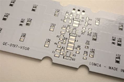
Introduction to AlN and Alumina Substrate Ceramic PCBs
Aluminum Nitride (AlN) and Alumina (Al2O3) are two popular ceramic materials used in the manufacturing of high-performance printed circuit boards (PCBs). These ceramic substrates offer unique properties that make them ideal for applications requiring excellent thermal conductivity, high electrical insulation, and superior mechanical stability. In this article, we will explore the characteristics, applications, and manufacturing process of AlN and Alumina substrate ceramic PCBs, as well as the benefits of choosing a one-stop manufacturing solution.
Characteristics of AlN and Alumina Substrates
Aluminum Nitride (AlN)
AlN is a ceramic material with exceptional thermal conductivity, making it an excellent choice for applications that require efficient heat dissipation. Some of the key characteristics of AlN include:
- High thermal conductivity (150-200 W/mK)
- High electrical resistivity (>10^14 Ω·cm)
- Low coefficient of thermal expansion (CTE) (4.5 ppm/°C)
- Good mechanical strength and stability
- Wide bandgap (6.2 eV), making it suitable for high-voltage applications
Alumina (Al2O3)
Alumina is another widely used ceramic substrate material, known for its excellent electrical insulation properties and mechanical strength. Key characteristics of Alumina include:
- High electrical resistivity (>10^14 Ω·cm)
- Moderate thermal conductivity (20-30 W/mK)
- High mechanical strength and hardness
- Good thermal stability
- Relatively low cost compared to other ceramic substrates
Applications of AlN and Alumina Substrate Ceramic PCBs
AlN and Alumina substrate ceramic PCBs find applications in various industries, including:
- Power electronics
- High-power LED lighting
- Automotive power modules
- Switching mode power supplies (SMPS)
-
Motor drives and inverters
-
RF and microwave devices
- 5G wireless communication
- Radar systems
- Satellite communication
-
Military and defense applications
-
Aerospace and aviation
- Avionics systems
- Satellite components
-
Radar and guidance systems
-
Medical devices
- High-frequency medical imaging equipment
- Implantable devices
-
Surgical instruments
-
Industrial automation and control
- Sensors and actuators
- Process control systems
- Power distribution and management
Manufacturing Process of AlN and Alumina Substrate Ceramic PCBs
The manufacturing process of AlN and Alumina substrate ceramic PCBs involves several critical steps to ensure high quality and reliability. Here’s an overview of the process:
1. Substrate Preparation
The first step in manufacturing ceramic PCBs is to prepare the AlN or Alumina substrate. This involves:
- Powder synthesis and processing
- Pressing and sintering the powder into a dense ceramic substrate
- Grinding and polishing the substrate surface to achieve the desired thickness and smoothness
2. Circuit Patterning
Once the substrate is prepared, the circuit pattern is created on the surface using various methods, such as:
- Screen printing: A conductive paste is applied through a patterned screen onto the substrate surface
- Photolithography: A photoresist layer is applied, exposed, and developed to create the desired circuit pattern
- Direct bonding: Thin metal foils (e.g., copper) are directly bonded to the substrate surface using high temperature and pressure
3. Via Formation
To create electrical connections between layers in multi-layer ceramic PCBs, vias (vertical interconnect access) are formed. Common methods include:
- Mechanical drilling
- Laser drilling
- Co-firing: Vias are formed during the substrate sintering process
4. Metallization
After the circuit pattern and vias are formed, the substrate undergoes metallization to create conductive traces and pads. This can be done using:
- Electroless plating: A thin layer of metal (e.g., copper) is deposited onto the substrate surface through a chemical reaction
- Electrolytic plating: Additional metal layers are deposited using an electric current to achieve the desired thickness
5. Surface Finish
To protect the metallized surface and improve solderability, a surface finish is applied. Common surface finishes for ceramic PCBs include:
- Gold (Au) plating
- Nickel (Ni) plating
- Nickel-Gold (Ni-Au) plating
- Silver (Ag) plating
6. Singulation and Packaging
Finally, the ceramic PCB Panel is singulated into individual boards using methods such as:
- Dicing
- Laser cutting
- Scribing and breaking
The individual boards are then packaged and shipped to the customer.

Benefits of One-Stop AlN and Alumina Ceramic PCB Manufacturing
Choosing a one-stop manufacturing solution for your AlN and Alumina substrate ceramic PCBs offers several advantages:
-
Streamlined process: A one-stop manufacturer handles all aspects of the production process, from substrate preparation to final packaging, reducing lead times and minimizing the risk of errors.
-
Cost-effectiveness: By consolidating all manufacturing steps under one roof, a one-stop solution can offer competitive pricing and help you save on logistics and transportation costs.
-
Quality control: A single manufacturer has complete control over the entire production process, ensuring consistent quality and adherence to strict standards.
-
Customization: One-stop manufacturers can work closely with you to develop custom designs and specifications tailored to your specific application requirements.
-
Technical support: With a one-stop solution, you have access to a team of experienced engineers and technicians who can provide expert guidance and support throughout the manufacturing process.

Comparison of AlN and Alumina Substrate Properties
| Property | AlN | Alumina (Al2O3) |
|---|---|---|
| Thermal Conductivity (W/mK) | 150-200 | 20-30 |
| Electrical Resistivity (Ω·cm) | >10^14 | >10^14 |
| Coefficient of Thermal Expansion (ppm/°C) | 4.5 | 6.5-7.5 |
| Mechanical Strength (MPa) | 300-400 | 300-500 |
| Dielectric Constant (@ 1 MHz) | 8.6-8.9 | 9.8-10.2 |
| Dielectric Loss (@ 1 MHz) | 0.001-0.002 | 0.0001-0.0002 |
| Density (g/cm³) | 3.26 | 3.90 |

Frequently Asked Questions (FAQ)
-
Q: What are the main differences between AlN and Alumina substrate ceramic PCBs?
A: AlN substrates offer higher thermal conductivity, lower CTE, and a wider bandgap compared to Alumina. Alumina substrates, on the other hand, have higher mechanical strength and are generally more cost-effective. -
Q: Can AlN and Alumina substrate ceramic PCBs be used for high-frequency applications?
A: Yes, both AlN and Alumina substrates are suitable for high-frequency applications due to their low dielectric loss and stable dielectric constant over a wide frequency range. -
Q: How do AlN and Alumina substrate ceramic PCBs compare to traditional FR-4 PCBs?
A: AlN and Alumina substrate ceramic PCBs offer superior thermal conductivity, electrical insulation, and mechanical stability compared to FR-4 PCBs. They are ideal for applications that require high power density, high-frequency operation, and reliable performance in harsh environments. -
Q: What are the typical lead times for AlN and Alumina substrate ceramic PCB manufacturing?
A: Lead times for AlN and Alumina substrate ceramic PCBs can vary depending on the complexity of the design, the quantity ordered, and the manufacturer’s capacity. Typical lead times range from 4 to 8 weeks, but expedited services may be available for urgent requirements. -
Q: How can I choose the right ceramic substrate material for my application?
A: The choice between AlN and Alumina substrates depends on your specific application requirements. Consider factors such as thermal management needs, electrical performance, mechanical stability, and budget constraints. Consult with a knowledgeable ceramic PCB Manufacturer to discuss your requirements and receive expert guidance on substrate material selection.
Conclusion
AlN and Alumina substrate ceramic PCBs offer unique properties that make them ideal for high-performance applications in various industries, including power electronics, RF and microwave devices, aerospace, medical devices, and industrial automation. By understanding the characteristics, manufacturing process, and benefits of these ceramic substrates, engineers and designers can make informed decisions when selecting the right material for their projects.
Choosing a one-stop manufacturing solution for your AlN and Alumina substrate ceramic PCBs can streamline the production process, ensure consistent quality, and provide access to expert technical support. With the growing demand for high-performance electronics in challenging environments, AlN and Alumina substrate ceramic PCBs are set to play an increasingly important role in shaping the future of advanced technology.
No responses yet