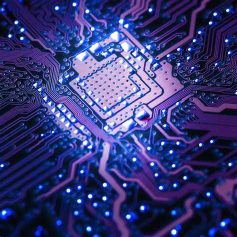
Introduction to High Current PCB Design
High current PCB design is a specialized area of printed circuit board design that focuses on the efficient and safe handling of high electrical currents. As electronic devices become more powerful and compact, the demand for PCBs capable of managing higher currents continues to grow. Designing a high current PCB requires careful consideration of various factors, such as trace width, copper thickness, thermal management, and component selection.
In this article, we will explore the key aspects of high current PCB design, including best practices, common challenges, and solutions to ensure optimal performance and reliability.
Understanding High Current PCB Applications
High current PCBs find applications in a wide range of industries and devices, including:
- Power electronics
- Automotive systems
- Industrial control systems
- Telecommunications equipment
- High-power LED lighting
These applications often require PCBs to handle currents ranging from several amperes to hundreds of amperes, depending on the specific requirements of the device or system.

Key Considerations in High Current PCB Design
Trace Width and Copper Thickness
One of the most critical aspects of high current PCB design is determining the appropriate trace width and copper thickness. The trace width and copper thickness directly impact the current-carrying capacity of the PCB traces. Wider traces and thicker copper layers allow for higher current flow without excessive heating or voltage drop.
To calculate the required trace width, designers can use online calculators or refer to industry standards, such as the IPC-2221 standard. The following table provides a general guideline for trace width based on current requirements and copper thickness:
| Current (A) | Copper Thickness (oz) | Trace Width (mm) |
|---|---|---|
| 1 | 1 | 0.25 |
| 5 | 1 | 1.25 |
| 10 | 2 | 2.50 |
| 20 | 2 | 5.00 |
| 50 | 4 | 12.50 |
Thermal Management
High current PCBs generate significant amounts of heat due to the large currents flowing through the traces. Proper thermal management is essential to prevent overheating, which can lead to component failure and reduced PCB lifespan. Some techniques for effective thermal management include:
- Using a larger copper area for high-current traces to dissipate heat more efficiently
- Incorporating thermal vias to transfer heat from the PCB surface to the inner layers or ground plane
- Selecting components with appropriate power ratings and thermal characteristics
- Implementing heat sinks or cooling fans for critical components
Component Selection
Choosing the right components is crucial for high current PCB design. Components must be rated for the expected current levels and should have low resistance to minimize power loss and heat generation. Some key components to consider include:
- Power connectors with adequate current ratings
- High-current capacitors and inductors
- Power MOSFETs or IGBTs with low on-resistance
- Current sense resistors with low resistance and high power ratings
PCB Layer Stack-up
The PCB layer stack-up plays a significant role in high current design. A well-designed stack-up can help distribute current evenly, minimize resistance, and improve heat dissipation. Some best practices for high current PCB layer stack-up include:
- Using thicker copper layers for power and ground planes
- Separating high-current traces from sensitive signals to reduce electromagnetic interference (EMI)
- Utilizing multiple power and ground layers to reduce impedance and improve current distribution

High Current PCB Layout Techniques
Star Ground Topology
The star ground topology is a common technique used in high current PCB layouts. This approach involves creating a central ground point (star point) and connecting all ground traces to it. The star ground topology helps minimize ground loops and reduces the overall ground impedance, which is essential for maintaining signal integrity and reducing EMI.
Kelvin Sensing
Kelvin sensing is a technique used to accurately measure voltage across a high-current component, such as a shunt resistor. By using separate traces for current-carrying and voltage-sensing paths, Kelvin sensing minimizes the impact of trace resistance on voltage measurements. This technique is particularly useful in power monitoring and control applications.
Current Density and Trace Spacing
Designers must consider current density and trace spacing when routing high-current traces on a PCB. Current density refers to the amount of current flowing per unit area of the trace cross-section. Exceeding the maximum current density can lead to excessive heating and potential trace failure.
Trace spacing is also important to prevent arcing and ensure proper insulation between high-current traces. The following table provides a general guideline for trace spacing based on voltage levels:
| Voltage (V) | Minimum Trace Spacing (mm) |
|---|---|
| 50 | 0.8 |
| 100 | 1.5 |
| 200 | 3.0 |
| 500 | 7.5 |

Testing and Validation of High Current PCBs
Once the high current PCB design is complete, thorough testing and validation are essential to ensure the board meets the required specifications and can handle the expected current levels reliably. Some common tests for high current PCBs include:
- Current-carrying capacity tests
- Thermal imaging to identify hot spots
- Voltage drop measurements
- Insulation resistance tests
- EMI/EMC tests
Proper testing and validation help identify potential issues early in the development process, reducing the risk of costly redesigns or field failures.
Frequently Asked Questions (FAQ)
-
What is the difference between trace width and copper thickness in high current PCB design?
Trace width refers to the width of the copper trace on the PCB surface, while copper thickness refers to the thickness of the copper layer. Both trace width and copper thickness contribute to the current-carrying capacity of the trace. -
How do I select the appropriate components for a high current PCB?
When selecting components for a high current PCB, consider the expected current levels, power ratings, and thermal characteristics. Choose components with low resistance and adequate current ratings to minimize power loss and heat generation. -
What is the purpose of thermal vias in high current PCB design?
Thermal vias are used to transfer heat from the PCB surface to the inner layers or ground plane. They help dissipate heat more efficiently, preventing overheating and improving the overall thermal performance of the PCB. -
What is star ground topology, and why is it used in high current PCB layouts?
Star ground topology involves creating a central ground point (star point) and connecting all ground traces to it. This technique minimizes ground loops and reduces the overall ground impedance, which is essential for maintaining signal integrity and reducing EMI in high current PCBs. -
Why is testing and validation important for high current PCBs?
Testing and validation are crucial for high current PCBs to ensure they meet the required specifications and can handle the expected current levels reliably. Thorough testing helps identify potential issues early in the development process, reducing the risk of costly redesigns or field failures.
Conclusion
High current PCB design is a complex and challenging task that requires careful consideration of various factors, such as trace width, copper thickness, thermal management, and component selection. By following best practices and utilizing appropriate design techniques, such as star ground topology and Kelvin sensing, designers can create PCBs that efficiently and safely handle high currents.
Furthermore, thorough testing and validation are essential to ensure the reliability and performance of high current PCBs in demanding applications. As electronic devices continue to push the boundaries of power and performance, the importance of well-designed high current PCBs will only continue to grow.
No responses yet