What are Printed Circuit Boards (PCBs)?
PCBs are flat boards made of insulating materials, such as fiberglass or plastic, with conductive pathways etched or printed onto their surface. These pathways, known as traces, connect various electronic components, such as resistors, capacitors, and integrated circuits (ICs), to form a complete electronic circuit.
Types of PCBs
There are several types of PCBs, each designed to meet specific requirements and applications:
-
Single-sided PCBs: These boards have conductive traces on only one side of the insulating substrate. They are the simplest and most cost-effective type of PCB, suitable for low-complexity circuits.
-
Double-sided PCBs: These boards have conductive traces on both sides of the insulating substrate, allowing for more complex circuits and higher component density. The two sides are connected using through-hole technology or vias.
-
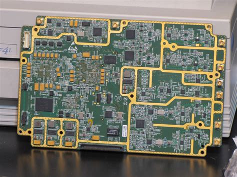
Multi-layer PCBs: These boards consist of multiple layers of insulating substrates with conductive traces sandwiched between them. They offer the highest level of complexity and component density, making them ideal for advanced electronic applications.
-
Flexible PCBs: These boards are made of flexible insulating materials, such as polyimide, allowing them to bend and conform to various shapes. They are commonly used in wearable electronics, medical devices, and aerospace applications.
-
Rigid-Flex PCBs: These boards combine the features of rigid and flexible PCBs, offering both stability and flexibility in a single board. They are often used in applications that require high reliability and complex packaging.
History of PCBs
The development of PCBs can be traced back to the early 20th century, with several key milestones:
-
1903: Albert Hanson, a German inventor, files a patent for a “printed wire” board, which laid the foundation for modern PCBs.
-
1936: Paul Eisler, an Austrian engineer, develops the first operational printed circuit board for a radio set.
-
1943: The United States military adopts PCBs for use in proximity fuses during World War II, greatly accelerating their development and production.
-
1950s: The introduction of through-hole technology and the development of soldering techniques enable the mass production of PCBs.
-
1960s: The advent of Surface-Mount Technology (SMT) allows for smaller components and higher component density on PCBs.
-
1980s: The development of multi-layer PCBs and the introduction of computer-aided design (CAD) software revolutionize PCB design and manufacturing.
-
1990s-Present: Advancements in materials, manufacturing processes, and design tools continue to drive the evolution of PCBs, enabling the development of increasingly complex and miniaturized electronic devices.

PCB Manufacturing Process
The PCB manufacturing process involves several key steps:
1. PCB Design
The PCB design process begins with creating a schematic diagram that represents the electronic circuit. This schematic is then translated into a physical layout using CAD software, which determines the placement of components and the routing of conductive traces.
2. PCB Fabrication
Once the PCB design is finalized, the fabrication process begins:
-
Substrate preparation: The insulating substrate, typically made of fiberglass or plastic, is cut to the desired size and shape.
-
Copper lamination: A thin layer of copper foil is laminated onto the substrate using heat and pressure.
-
Photoresist application: A photosensitive resist is applied to the copper layer and exposed to UV light through a photomask, which contains the PCB layout pattern.
-
Etching: The exposed copper is etched away using a chemical solution, leaving only the desired conductive traces.
-
Drilling: Holes are drilled through the board to accommodate through-hole components and create vias for multi-layer PCBs.
-
Plating: The holes are plated with copper to create electrical connections between layers.
-
Solder mask application: A protective solder mask is applied to the board, exposing only the areas where components will be soldered.
-
Silkscreen printing: A silkscreen layer is printed onto the board to add text, logos, and component identifiers.
-
Surface finishing: A surface finish, such as HASL (Hot Air Solder Leveling) or ENIG (Electroless Nickel Immersion Gold), is applied to protect the exposed copper and enhance solderability.
3. PCB Assembly
After the PCB is fabricated, the electronic components are assembled onto the board:
-
Solder paste application: Solder paste is applied to the pads where components will be placed using a stencil or screen printing process.
-
Component placement: Components are placed onto the board using automated pick-and-place machines or manual assembly for low-volume production.
-
Reflow soldering: The board is heated in a reflow oven, melting the solder paste and creating a permanent electrical and mechanical connection between the components and the PCB.
-
Inspection and testing: The assembled PCB undergoes visual inspection and electrical testing to ensure proper functionality and quality control.

Applications of PCBs
PCBs are used in a wide range of industries and applications, including:
-
Consumer electronics: Smartphones, tablets, laptops, televisions, and home appliances.
-
Automotive: Engine control units, infotainment systems, and advanced driver assistance systems (ADAS).
-
Medical devices: Diagnostic equipment, patient monitoring systems, and implantable devices.
-
Aerospace and defense: Avionics, satellites, and military communication systems.
-
Industrial automation: Process control systems, robotics, and machine vision.
-
Telecommunications: Networking equipment, base stations, and fiber optic systems.
-
Internet of Things (IoT): Smart home devices, wearables, and sensor networks.
| Application | Examples |
|---|---|
| Consumer electronics | Smartphones, tablets, laptops, televisions, home appliances |
| Automotive | Engine control units, infotainment systems, advanced driver assistance systems (ADAS) |
| Medical devices | Diagnostic equipment, patient monitoring systems, implantable devices |
| Aerospace and defense | Avionics, satellites, military communication systems |
| Industrial automation | Process control systems, robotics, machine vision |
| Telecommunications | Networking equipment, base stations, fiber optic systems |
| Internet of Things | Smart home devices, wearables, sensor networks |

Future Trends in PCB Technology
As electronic devices continue to evolve, so do PCBs. Some of the key trends shaping the future of PCB technology include:
-
Miniaturization: The demand for smaller, more compact electronic devices is driving the development of advanced PCB manufacturing techniques, such as embedded components and 3D printing.
-
High-speed applications: The increasing bandwidth requirements of modern electronics are pushing the limits of PCB design and materials, leading to the development of low-loss substrates and advanced signal integrity techniques.
-
Flexible and wearable electronics: The growth of the wearable technology market is driving the adoption of flexible and stretchable PCBs, enabling the integration of electronics into clothing, accessories, and medical devices.
-
Sustainability: As environmental concerns grow, the PCB industry is focusing on developing eco-friendly materials and processes, such as halogen-free substrates and lead-free solders.
-
Intelligent PCBs: The integration of sensors, microcontrollers, and wireless connectivity into PCBs is enabling the development of smart, connected devices that can collect, process, and transmit data.
Frequently Asked Questions (FAQ)
-
Q: What is the difference between a PCB and a Printed Wiring Board (PWB)?
A: PCB and PWB are often used interchangeably, but historically, PWBs referred to boards with through-hole technology, while PCBs encompassed both through-hole and surface-mount technology. -
Q: What are the most common materials used for PCB substrates?
A: The most common PCB substrate materials are FR-4 (a type of fiberglass), polyimide, and PTFE (polytetrafluoroethylene, also known as Teflon). -
Q: How do I choose the right type of PCB for my application?
A: The choice of PCB type depends on factors such as circuit complexity, component density, operating environment, and budget. Consult with a PCB manufacturer or design engineer to determine the most suitable type for your specific application. -
Q: What is the typical turnaround time for PCB manufacturing?
A: The turnaround time for PCB manufacturing varies depending on the complexity of the design, the chosen fabrication techniques, and the manufacturer’s capacity. Simple PCBs can be produced in a few days, while complex, multi-layer boards may take several weeks. -
Q: How can I ensure the quality and reliability of my PCBs?
A: To ensure PCB Quality and reliability, follow best practices in design, such as adhering to manufacturer guidelines, conducting thorough design reviews, and specifying appropriate testing and inspection procedures. Choose a reputable PCB manufacturer with a proven track record of quality and reliability.
In conclusion, PCBs play a crucial role in the modern electronics industry, enabling the development of increasingly complex, compact, and reliable devices across a wide range of applications. As technology continues to advance, PCBs will remain at the forefront of innovation, driving the future of electronics and shaping our world in countless ways.
No responses yet