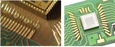
Introduction to PCB Metallization
Printed Circuit Boards (PCBs) are the backbone of modern electronics. They provide a reliable and efficient way to connect electronic components and create complex circuits. One of the critical aspects of PCB manufacturing is metallization, which involves depositing a thin layer of metal on the surface of the board. This metal layer serves as a conductive pathway for electrical signals and helps to protect the board from corrosion and wear.
Silver and gold are two of the most commonly used metals in PCB metallization. In this article, we will explore the reasons why these precious metals are preferred in electronic circuits and how they contribute to building a basic PCB Board.
The Role of Metallization in PCB Manufacturing
Metallization is a crucial step in the PCB manufacturing process. It involves depositing a thin layer of metal on the surface of the board, typically using a process called electroplating. The metal layer serves several important functions:
-
Conductivity: The metal layer provides a low-resistance pathway for electrical signals to travel between components on the board.
-
Protection: The metal layer helps to protect the board from corrosion and wear, extending its lifespan and ensuring reliable performance over time.
-
Solderability: The metal layer provides a surface that is easy to solder components onto, ensuring a strong and reliable connection.
Common Metals Used in PCB Metallization
Several metals are commonly used in PCB metallization, each with its own unique properties and advantages. Some of the most popular choices include:
| Metal | Advantages | Disadvantages |
|---|---|---|
| Copper | – Excellent conductivity – Low cost – Easy to electroplate |
– Prone to oxidation – Requires additional protection |
| Nickel | – Good corrosion resistance – Provides a barrier between copper and other metals |
– Higher resistance than copper – Can cause allergic reactions |
| Gold | – Excellent corrosion resistance – High conductivity – Easy to solder |
– Expensive – Soft and prone to wear |
| Silver | – Highest conductivity of all metals – Good solderability |
– Expensive – Prone to tarnishing |

Why Silver and Gold are Preferred in Electronic Circuits
Despite their higher cost compared to other metals, silver and gold are often the preferred choice for PCB metallization in high-performance electronic circuits. There are several reasons for this:
Silver: The Ultimate Conductor
Silver is the most conductive metal on Earth, with a resistivity of just 1.59 x 10^-8 Ω·m at room temperature. This makes it an ideal choice for applications where low resistance and high conductivity are critical, such as in high-frequency circuits or power electronics.
Silver also has excellent solderability, meaning that components can be easily and reliably attached to silver-plated surfaces. This is particularly important in applications where a strong and stable connection is essential, such as in aerospace or medical devices.
Gold: The King of Corrosion Resistance
Gold is well known for its resistance to corrosion and oxidation. Unlike other metals, gold does not react with oxygen or most other chemicals, making it an ideal choice for applications where reliability and longevity are paramount.
Gold is also an excellent conductor, with a resistivity of just 2.44 x 10^-8 Ω·m at room temperature. While not quite as conductive as silver, gold’s corrosion resistance and durability make it a popular choice for high-end electronics.
Combining Silver and Gold for Optimal Performance
In some cases, PCB manufacturers may choose to use a combination of silver and gold in their metallization processes. For example, a board may be plated with a layer of silver for its high conductivity, followed by a thin layer of gold for added corrosion resistance.
This combination of metals offers the best of both worlds: the high conductivity of silver and the durability and reliability of gold. It is often used in applications where performance and longevity are critical, such as in aerospace, military, or medical devices.

The PCB Metallization Process
The PCB metallization process typically involves several steps, each designed to ensure a high-quality, reliable metal layer on the surface of the board. These steps may include:
-
Cleaning: The board is thoroughly cleaned to remove any dirt, grease, or other contaminants that could interfere with the metallization process.
-
Activation: The surface of the board is treated with a chemical activator to improve adhesion of the metal layer.
-
Electroplating: The board is immersed in an electroplating bath containing the desired metal (such as silver or gold). An electric current is applied, causing the metal ions to bond to the surface of the board.
-
Rinsing: The board is rinsed with water to remove any excess plating solution.
-
Drying: The board is dried using heat or air to remove any remaining moisture.
-
Inspection: The board is inspected for quality and consistency, ensuring that the metal layer meets the required specifications.
Factors Affecting PCB Metallization Quality
Several factors can affect the quality and reliability of PCB metallization, including:
-
Surface preparation: Proper cleaning and activation of the board surface is essential for good adhesion of the metal layer.
-
Plating solution: The composition and purity of the plating solution can affect the quality and consistency of the metal layer.
-
Current density: The amount of electric current applied during electroplating can influence the thickness and uniformity of the metal layer.
-
Temperature: The temperature of the plating solution can affect the rate of metal deposition and the overall quality of the metal layer.
By carefully controlling these factors, PCB manufacturers can ensure a high-quality, reliable metal layer that meets the specific requirements of the application.

Benefits of Using Silver and Gold in PCB Metallization
Using silver and gold in PCB metallization offers several key benefits for electronic circuits:
-
Improved conductivity: The high conductivity of silver and gold allows for faster and more efficient transmission of electrical signals, reducing losses and improving overall circuit performance.
-
Enhanced durability: The corrosion resistance of gold helps to protect the board from damage caused by moisture, chemicals, or other environmental factors, extending the lifespan of the circuit.
-
Better solderability: Silver and gold both offer excellent solderability, ensuring strong and reliable connections between components and the board.
-
Higher reliability: The combination of high conductivity, corrosion resistance, and solderability makes silver and gold-plated circuits more reliable and stable over time, reducing the risk of failure or malfunction.
-
Compatibility with advanced components: As electronic components become smaller and more complex, the use of silver and gold in PCB metallization becomes increasingly important for ensuring compatibility and performance.
Challenges and Considerations
While silver and gold offer many benefits for PCB metallization, there are also some challenges and considerations to keep in mind:
-
Cost: Silver and gold are both precious metals and are more expensive than other commonly used metals such as copper or nickel. This can increase the overall cost of the PCB.
-
Availability: The limited supply of silver and gold can sometimes lead to availability issues or price fluctuations, which can impact PCB production.
-
Compatibility: Not all components or materials are compatible with silver or gold plating. In some cases, additional steps may be required to ensure proper adhesion or functionality.
-
Environmental concerns: The mining and processing of silver and gold can have negative environmental impacts, leading some manufacturers to seek out more sustainable alternatives.
Despite these challenges, the benefits of using silver and gold in PCB metallization often outweigh the drawbacks, particularly in high-performance or mission-critical applications.
Future Trends in PCB Metallization
As electronic devices continue to evolve and become more advanced, the demands on PCB metallization are also changing. Some of the key trends and developments to watch in the coming years include:
-
Miniaturization: As devices become smaller and more compact, PCB manufacturers will need to find ways to create thinner, more precise metal layers to accommodate smaller components and tighter tolerances.
-
High-frequency applications: The increasing use of high-frequency technologies such as 5G and millimeter-wave will require PCBs with even higher conductivity and lower losses, driving demand for advanced metallization techniques.
-
Sustainable materials: With growing concerns about the environmental impact of electronic waste, there is a growing interest in sustainable and recyclable PCB materials, including alternative metals or alloys for metallization.
-
Additive manufacturing: The use of additive manufacturing techniques such as 3D printing could enable new approaches to PCB metallization, such as selective plating or embedded conductors.
By staying ahead of these trends and continually innovating, PCB manufacturers can ensure that they are able to meet the evolving needs of the electronics industry.
Frequently Asked Questions
-
What is PCB metallization?
PCB metallization is the process of depositing a thin layer of metal onto the surface of a printed circuit board (PCB) to create conductive pathways and improve the board’s performance and durability. -
Why are silver and gold used in PCB metallization?
Silver and gold are used in PCB metallization because of their high conductivity, excellent corrosion resistance, and good solderability. These properties make them ideal for high-performance and mission-critical applications. -
How does PCB metallization affect circuit performance?
PCB metallization can improve circuit performance by providing low-resistance pathways for electrical signals, reducing losses and enabling faster and more efficient transmission. The use of high-conductivity metals like silver and gold can further enhance performance. -
What are some of the challenges associated with using silver and gold in PCB metallization?
Some of the challenges associated with using silver and gold in PCB metallization include higher cost compared to other metals, limited availability, potential compatibility issues with certain components or materials, and environmental concerns related to mining and processing. -
What are some of the future trends in PCB metallization?
Some of the key future trends in PCB metallization include miniaturization to accommodate smaller components, the use of advanced metallization techniques for high-frequency applications, the development of sustainable and recyclable materials, and the potential use of additive manufacturing techniques such as 3D printing.
Conclusion
PCB metallization is a critical process in the manufacturing of electronic circuits, providing the conductive pathways and protection needed for reliable and high-performance operation. The use of silver and gold in PCB metallization offers several key benefits, including high conductivity, excellent corrosion resistance, and good solderability.
While there are challenges and considerations associated with using these precious metals, the benefits often outweigh the drawbacks, particularly in high-performance or mission-critical applications. As electronic devices continue to evolve and become more advanced, PCB manufacturers will need to stay ahead of trends and continually innovate to meet the changing demands of the industry.
By understanding the role of metallization in PCB manufacturing and the specific advantages of silver and gold, engineers and designers can make informed decisions about the best materials and processes for their specific applications. With the right approach and expertise, PCB metallization can help to ensure the reliability, performance, and longevity of electronic circuits for years to come.
No responses yet