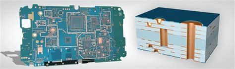
What are HDI PCBs?
HDI PCBs, or High Density Interconnector PCBs, are a type of printed circuit board that features a higher wiring density than traditional PCBs. This is achieved through the use of smaller vias, finer trace widths, and advanced manufacturing techniques. HDI PCBs can have trace widths and spaces as small as 50 microns (2 mil) and via diameters as small as 0.1 mm (4 mil).
The main characteristics of HDI PCBs include:
- Smaller vias (microvias) with diameters less than 0.15 mm (6 mil)
- Higher layer counts (typically 8 or more)
- Thin dielectric materials
- Fine line traces and spaces
- Buried and blind vias
Benefits of HDI PCBs
HDI PCBs offer several advantages over traditional PCBs, making them an attractive choice for a wide range of applications. Some of the key benefits include:
-
Increased component density: The smaller vias and finer trace widths of HDI PCBs allow for a higher component density, enabling more functionality to be packed into a smaller space.
-
Improved signal integrity: The shorter signal paths and reduced layer count of HDI PCBs result in improved signal integrity, reducing signal loss, crosstalk, and electromagnetic interference (EMI).
-
Reduced size and weight: The higher component density and smaller form factor of HDI PCBs enable the creation of smaller and lighter electronic devices.
-
Enhanced thermal management: HDI PCBs can incorporate advanced thermal management techniques, such as thermal vias and heat spreaders, to effectively dissipate heat generated by high-performance components.
-
Lower power consumption: The shorter signal paths in HDI PCBs result in lower power consumption, which is particularly beneficial for battery-powered devices.

HDI PCB Manufacturing Process
The manufacturing process for HDI PCBs is more complex than that of traditional PCBs due to the smaller features and tighter tolerances involved. The key steps in the HDI PCB manufacturing process include:
-
Material selection: Choosing the right base material and copper foil is crucial for HDI PCBs. Common base materials include FR-4, polyimide, and Rogers materials, while copper foil thicknesses range from 9 to 35 microns (0.35 to 1.4 mil).
-
Drilling: Mechanical drilling is used to create through-holes, while laser drilling is used for microvias. Laser drilling enables the creation of smaller, more precise vias.
-
Patterning: The circuit pattern is transferred onto the PCB using photolithography and etching processes. HDI PCBs require high-resolution photomasks and precise alignment to achieve the fine features.
-
Lamination: The PCB Layers are laminated together using heat and pressure, with special care taken to ensure proper registration of the layers.
-
Plating: The vias and through-holes are plated with copper to establish electrical connections between layers.
-
Surface finish: A surface finish, such as ENIG (Electroless Nickel Immersion Gold) or HASL (Hot Air Solder Leveling), is applied to protect the copper and enhance solderability.
-
Electrical testing: The finished HDI PCB undergoes rigorous electrical testing to ensure proper functionality and adherence to specifications.

HDI PCB Design Considerations
Designing HDI PCBs requires careful consideration of several factors to ensure optimal performance and manufacturability. Some key design considerations include:
-
Layer stack-up: The arrangement of the layers in an HDI PCB is critical for signal integrity and manufacturability. The layer stack-up should be designed to minimize signal crosstalk and EMI while ensuring proper impedance control.
-
Via types and placement: HDI PCBs can incorporate various types of vias, including through-hole, blind, buried, and microvias. The choice and placement of vias should be optimized for signal integrity, manufacturability, and cost.
-
Trace width and spacing: The fine trace widths and spacing of HDI PCBs require careful design to ensure proper signal integrity and manufacturability. Designers must adhere to the manufacturer’s design rules and guidelines.
-
Component placement: The high component density of HDI PCBs necessitates careful component placement to minimize signal path lengths, avoid signal integrity issues, and ensure adequate thermal management.
-
Signal integrity analysis: Signal integrity analysis, including impedance control and crosstalk analysis, should be performed to ensure optimal signal quality and minimize signal distortion.

Applications of HDI PCBs
HDI PCBs are used in a wide range of applications that require high performance, small form factors, and advanced functionality. Some common applications include:
-
Consumer electronics: Smartphones, tablets, wearables, and other portable devices.
-
Automotive electronics: Advanced driver assistance systems (ADAS), infotainment systems, and vehicle control modules.
-
Medical devices: Implantable devices, diagnostic equipment, and patient monitoring systems.
-
Aerospace and defense: Avionics, radar systems, and satellite communications equipment.
-
Industrial automation: Robotics, machine vision systems, and process control equipment.
RAYPCB’s HDI PCB Capabilities
RAYPCB is a leading provider of high-quality HDI PCBs, offering a full range of services from design to manufacturing. Some of RAYPCB’s key HDI PCB capabilities include:
-
Advanced manufacturing facilities: RAYPCB’s state-of-the-art manufacturing facilities are equipped with the latest equipment and technologies to produce HDI PCBs with the highest quality and reliability.
-
Experienced engineering team: RAYPCB’s team of experienced engineers provides expert support throughout the entire HDI PCB design and manufacturing process, ensuring optimal results.
-
Rapid prototyping: RAYPCB offers fast turnaround times for HDI PCB Prototypes, enabling customers to quickly test and refine their designs.
-
Flexible manufacturing options: RAYPCB can accommodate a wide range of HDI PCB specifications, including various layer counts, materials, and surface finishes.
-
Stringent quality control: RAYPCB employs rigorous quality control measures, including automated optical inspection (AOI), X-ray inspection, and electrical testing, to ensure the highest quality standards are met.
Frequently Asked Questions (FAQ)
-
What is the minimum feature size for HDI PCBs?
The minimum feature size for HDI PCBs varies depending on the manufacturer’s capabilities. RAYPCB can produce HDI PCBs with trace widths and spaces as small as 50 microns (2 mil) and via diameters as small as 0.1 mm (4 mil). -
What are the benefits of using microvias in HDI PCBs?
Microvias offer several benefits, including higher component density, shorter signal paths, and improved signal integrity. They also enable the creation of more complex layer stack-ups and the use of advanced packaging technologies. -
What materials are commonly used for HDI PCBs?
Common base materials for HDI PCBs include FR-4, polyimide, and Rogers materials. The choice of material depends on the specific application requirements, such as thermal performance, dielectric constant, and loss tangent. -
How do HDI PCBs differ from traditional PCBs?
HDI PCBs differ from traditional PCBs in several ways, including smaller vias, finer trace widths and spaces, higher layer counts, and the use of advanced manufacturing techniques. These differences enable HDI PCBs to offer higher performance, smaller form factors, and advanced functionality. -
What should I consider when choosing an HDI PCB Manufacturer?
When choosing an HDI PCB manufacturer, consider factors such as the manufacturer’s experience, capabilities, quality control measures, and customer support. It’s also important to ensure that the manufacturer can accommodate your specific design requirements and provide competitive pricing and lead times.
Conclusion
HDI PCBs are a crucial technology for meeting the growing demands of today’s electronics industry. By offering higher component density, improved signal integrity, and reduced size and weight, HDI PCBs enable the creation of smaller, faster, and more powerful devices. RAYPCB, with its advanced manufacturing capabilities, experienced engineering team, and commitment to quality, is well-positioned to meet the HDI PCB needs of customers across a wide range of industries.
As the electronics industry continues to evolve, the importance of HDI PCBs will only continue to grow. By partnering with a trusted and experienced HDI PCB manufacturer like RAYPCB, companies can stay at the forefront of this exciting technology and deliver cutting-edge products to their customers.
| Feature | Traditional PCBs | HDI PCBs |
|---|---|---|
| Trace width/space | ≥ 100 µm (4 mil) | ≥ 50 µm (2 mil) |
| Via diameter | ≥ 0.3 mm (12 mil) | ≥ 0.1 mm (4 mil) |
| Layer count | Typically ≤ 8 | Typically ≥ 8 |
| Via types | Through-hole | Through-hole, blind, buried, microvia |
| Manufacturing complexity | Lower | Higher |
In summary, HDI PCBs represent a significant advancement in PCB technology, offering numerous benefits over traditional PCBs. With their ability to enable smaller, faster, and more powerful electronic devices, HDI PCBs are poised to play an increasingly important role in shaping the future of the electronics industry. As a leader in HDI PCB manufacturing, RAYPCB is committed to helping its customers harness the full potential of this exciting technology.
No responses yet