Understanding PCB Thickness
What is PCB Thickness?
PCB thickness refers to the overall height of the printed circuit board, including the core substrate, copper layers, solder mask, and silkscreen. The thickness is typically measured in millimeters (mm) or mils (thousandths of an inch). Standard PCB thicknesses range from 0.4mm to 3.2mm, with 1.6mm being the most common.
Factors Affecting PCB Thickness Choice
Several factors come into play when deciding on the appropriate PCB thickness for your prototype. These include:
- Application requirements
- Layer count
- Mechanical strength
- Thermal management
- Manufacturing constraints
- Cost considerations
Let’s dive deeper into each of these factors.
Application Requirements
Electrical Performance
The electrical performance of your PCB Prototype is a primary consideration when choosing the thickness. High-speed and high-frequency applications often require thinner PCBs to minimize signal distortion and maintain signal integrity. Thinner boards allow for shorter signal paths, reducing the risk of signal reflection and crosstalk.
Physical Dimensions
The physical dimensions of your PCB prototype also play a role in thickness selection. If your design needs to fit into a specific enclosure or has limited space constraints, a thinner PCB may be necessary. On the other hand, if your prototype requires additional mechanical support or needs to withstand harsh environments, a thicker PCB may be more suitable.
Flexibility
In some cases, your PCB prototype may require a certain degree of flexibility. Flexible PCBs are typically thinner than rigid PCBs, allowing them to bend and conform to various shapes. If your application demands flexibility, you may need to opt for a thinner PCB substrate.

Layer Count
Single-Layer PCBs
Single-layer PCBs consist of a single conductive layer, typically made of copper, bonded to a non-conductive substrate. These PCBs are the thinnest and most cost-effective option, with thicknesses ranging from 0.4mm to 0.8mm. Single-layer PCBs are suitable for simple, low-density designs with minimal components.
Double-Layer PCBs
Double-layer PCBs have two conductive layers, one on each side of the substrate. They offer more flexibility in terms of component placement and routing compared to single-layer PCBs. Double-layer PCBs are commonly used for moderate-complexity designs and have thicknesses ranging from 0.8mm to 1.6mm.
Multi-Layer PCBs
Multi-layer PCBs consist of three or more conductive layers, separated by insulating layers. As the number of layers increases, so does the thickness of the PCB. Multi-layer PCBs are used for complex, high-density designs that require intricate routing and signal integrity. The thickness of multi-layer PCBs can range from 1.6mm to 3.2mm or more, depending on the number of layers and the specific application requirements.
Here’s a table summarizing the typical thicknesses for different layer counts:
| Layer Count | Typical Thickness Range |
|---|---|
| Single-layer | 0.4mm – 0.8mm |
| Double-layer | 0.8mm – 1.6mm |
| 4-layer | 1.6mm – 2.0mm |
| 6-layer | 2.0mm – 2.4mm |
| 8-layer | 2.4mm – 3.2mm |

Mechanical Strength
Substrate Material
The choice of substrate material directly affects the mechanical strength of your PCB prototype. The most common substrate materials are:
- FR-4: A glass-reinforced epoxy laminate, FR-4 is the most widely used substrate material. It offers good mechanical strength, electrical insulation, and thermal stability.
- Aluminum: Aluminum PCBs provide excellent thermal dissipation and mechanical stability. They are often used in high-power applications or where heat management is critical.
- Flexible substrates: Flexible PCBs use materials like polyimide or polyester, which are thinner and more flexible than rigid substrates. They offer reduced mechanical strength but enable bendable and conformable designs.
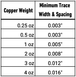
Copper Weight
The copper weight, measured in ounces per square foot (oz/ft²), also contributes to the mechanical strength of your PCB prototype. Higher copper weights provide better mechanical stability but can increase the overall thickness of the board. Common copper weights include 0.5 oz/ft², 1 oz/ft², and 2 oz/ft².
Reinforcement Techniques
In applications that require enhanced mechanical strength, additional reinforcement techniques can be employed. These include:
- Using thicker substrates: Increasing the thickness of the substrate can improve the mechanical rigidity of the PCB.
- Adding support structures: Incorporating support structures, such as stiffeners or frames, can provide additional mechanical support to the PCB.
- Using high-strength materials: Selecting high-strength substrate materials, such as high-Tg FR-4 or metal-core substrates, can enhance the mechanical performance of the PCB.

Thermal Management
Thermal Conductivity
The thermal conductivity of the PCB substrate plays a crucial role in heat dissipation. PCBs with better thermal conductivity can efficiently transfer heat away from components, preventing overheating and ensuring reliable operation. Thicker PCBs generally have better thermal conductivity compared to thinner ones, as they provide more mass for heat dissipation.
Copper Thickness
Increasing the copper thickness can also improve thermal management in your PCB prototype. Thicker copper layers provide more surface area for heat dissipation and can handle higher current carrying capacity. However, increasing copper thickness also increases the overall thickness of the PCB.
Thermal Vias
Thermal vias are small, plated holes drilled through the PCB to transfer heat from one layer to another. They help in dissipating heat away from hot spots on the board. Incorporating thermal vias can enhance thermal management without significantly increasing the PCB thickness.
Manufacturing Constraints
Minimum Thickness Limits
PCB manufacturers have minimum thickness limitations based on their production capabilities and equipment. It’s essential to consult with your manufacturer to understand their minimum thickness requirements. Attempting to produce PCBs thinner than the manufacturer’s limits can lead to production issues and reduced yields.
Aspect Ratio
The aspect ratio is the ratio of the PCB thickness to the smallest drilled hole diameter. A higher aspect ratio can make it challenging to produce reliable plated through-holes and vias. Manufacturers typically specify a maximum aspect ratio they can accommodate. When designing your PCB prototype, ensure that the selected thickness and hole sizes fall within the manufacturer’s aspect ratio guidelines.
Stackup Considerations
The PCB stackup refers to the arrangement of layers and materials within the board. The stackup design can impact the thickness of your PCB prototype. Factors such as the number of layers, dielectric thickness, and copper weight all contribute to the overall thickness. Work closely with your manufacturer to optimize the stackup design while meeting your thickness requirements.
Cost Considerations
Material Costs
The cost of your PCB prototype is influenced by the choice of materials, including the substrate and copper thickness. Thicker PCBs generally require more material, which can increase the overall cost. However, it’s important to balance cost savings with the necessary performance and reliability requirements of your application.
Manufacturing Costs
PCB thickness can also impact manufacturing costs. Thinner PCBs may require specialized equipment and processes, which can increase production costs. On the other hand, thicker PCBs may necessitate additional drilling and plating steps, also affecting the manufacturing cost. Discuss the cost implications of different thickness options with your manufacturer to make an informed decision.
Frequently Asked Questions (FAQ)
-
Q: What is the most common PCB thickness?
A: The most common PCB thickness is 1.6mm (0.063 inches). This thickness provides a good balance between mechanical strength, thermal management, and manufacturing feasibility for a wide range of applications. -
Q: Can I use a thinner PCB to reduce costs?
A: While using a thinner PCB may reduce material costs, it’s essential to consider the impact on performance and reliability. Thinner PCBs may be more susceptible to mechanical stress, thermal issues, and manufacturing challenges. It’s recommended to consult with your manufacturer and carefully evaluate the trade-offs before opting for a thinner PCB solely for cost reduction. -
Q: How does PCB thickness affect signal integrity?
A: PCB thickness can influence signal integrity, particularly in high-speed and high-frequency applications. Thinner PCBs allow for shorter signal paths, which can minimize signal distortion and improve signal integrity. However, thinner PCBs may also be more susceptible to crosstalk and electromagnetic interference (EMI) if not designed properly. -
Q: Can I mix different thicknesses within the same PCB?
A: Yes, it is possible to have different thicknesses within the same PCB, known as a stepped or sculpted PCB. This technique involves selectively removing or adding layers in specific areas of the board to achieve different thicknesses. Stepped PCBs can be useful in applications that require varying levels of mechanical strength or thermal management in different regions of the board. -
Q: How do I determine the appropriate PCB thickness for my prototype?
A: To determine the appropriate PCB thickness for your prototype, consider the following factors: - Evaluate the electrical performance requirements, including signal integrity and power management.
- Assess the mechanical requirements, such as strength, stiffness, and flexibility.
- Consider the thermal management needs, especially for high-power applications.
- Review the manufacturing constraints and capabilities of your chosen PCB manufacturer.
- Analyze the cost implications of different thickness options.
By carefully evaluating these factors and consulting with your PCB manufacturer, you can make an informed decision on the optimal thickness for your PCB prototype.
Conclusion
Choosing the correct thickness for your PCB prototype is a critical decision that impacts the performance, reliability, and cost of your design. By understanding the factors that influence PCB thickness, such as application requirements, layer count, mechanical strength, thermal management, manufacturing constraints, and cost considerations, you can make an informed choice.
Remember to collaborate closely with your PCB manufacturer throughout the design process. They can provide valuable insights and guidance based on their expertise and manufacturing capabilities. By selecting the appropriate PCB thickness and optimizing your design accordingly, you can ensure the success of your PCB prototype and final product.
No responses yet