What is QFP Solder Bridging?
Solder bridging occurs when excess solder accidentally connects two or more adjacent pins on a QFP component, creating an unintended electrical connection. This can lead to short circuits, malfunctions, and even permanent damage to the device.
Causes of QFP Solder Bridging
There are several factors that can contribute to the occurrence of solder bridging in QFP components:
- Excessive solder paste
- Improper solder paste stencil design
- Inadequate solder paste printing process
- Incorrect reflow profile
- Poor component placement
- Insufficient cleaning of the PCB before soldering
Solutions to Prevent QFP Solder Bridging
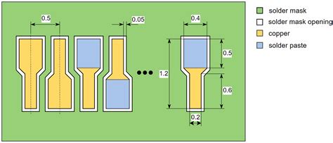
1. Optimize Solder Paste Stencil Design
The solder paste stencil plays a crucial role in the soldering process. Ensure that the stencil apertures are correctly sized and positioned to match the QFP pad layout. Consider the following factors when designing the stencil:
- Aperture size: The aperture should be slightly smaller than the pad size to prevent excessive solder paste deposition.
- Aperture shape: Use rectangular or home plate-shaped apertures for QFP pads to improve solder paste release and reduce the risk of bridging.
- Stencil thickness: Choose an appropriate stencil thickness based on the pad size and pitch of the QFP component. A typical thickness range is 0.1mm to 0.15mm.
2. Control Solder Paste Printing Process
Proper solder paste printing is essential to achieve reliable solder joints and minimize bridging. Follow these guidelines:
- Use a high-quality solder paste with the appropriate particle size and flux activity for your application.
- Ensure that the solder paste is at room temperature before printing to maintain consistent viscosity.
- Regularly clean and maintain the stencil to prevent clogged apertures and uneven paste deposition.
- Optimize the printing parameters, such as squeegee pressure, speed, and angle, to achieve uniform paste coverage.
3. Implement Correct Reflow Profile
The reflow profile determines the temperature and duration of the soldering process. An incorrect reflow profile can lead to solder bridging and other defects. Consider these points:
- Follow the manufacturer’s recommended reflow profile for the specific solder paste and QFP component.
- Ensure that the peak temperature and time above liquidus (TAL) are within the specified range.
- Avoid excessive temperature ramp rates, which can cause solder splatter and bridging.
- Optimize the cooling rate to allow proper solder joint formation and minimize thermal stress on the components.
4. Ensure Accurate Component Placement
Precise placement of QFP components is critical to prevent solder bridging. Use the following techniques:
- Employ high-precision pick-and-place machines with vision systems for accurate component alignment.
- Verify the placement accuracy and adjust the machine settings if necessary.
- Use appropriate nozzles and placement force to avoid damaging the component leads or disturbing the solder paste.
5. Clean PCB Before Soldering
Contaminants on the PCB surface, such as dust, grease, or oxidation, can interfere with the soldering process and promote bridging. Ensure proper PCB Cleaning:
- Clean the PCB with isopropyl alcohol or a specialized PCB cleaner before solder paste printing.
- Use an ionizer to neutralize static charges and prevent the attraction of dust particles.
- Handle the PCB with gloves to avoid introducing oils and contaminants from skin contact.
6. Utilize Solder Masks and Flux Barriers
Solder masks and flux barriers can help contain the solder paste and prevent bridging. Consider these options:
- Apply a solder mask on the PCB to define the solderable areas and prevent solder from spreading to undesired locations.
- Use flux barriers, such as dams or wells, around the QFP pads to restrict the flow of solder paste during reflow.
7. Implement Inspection and Rework Procedures
Despite taking preventive measures, solder bridging may still occur. Implement thorough inspection and rework procedures:
- Conduct visual inspection of the soldered QFP components using magnification or automated optical inspection (AOI) systems.
- Use x-ray inspection for hidden solder joints or to detect bridging underneath the component.
- If bridging is detected, carefully remove the excess solder using a soldering iron with a fine tip or a solder sucker.
- Clean the area thoroughly after rework to remove any residual flux or debris.

FAQ
1. What is the most common cause of QFP solder bridging?
The most common cause of QFP solder bridging is excessive solder paste deposition, often due to improper stencil design or printing process.
2. Can solder bridging be detected visually?
Yes, solder bridging can often be detected visually using magnification or automated optical inspection (AOI) systems. However, some bridges may be hidden underneath the component and require x-ray inspection.
3. How can I remove solder bridges without damaging the component?
To remove solder bridges, use a soldering iron with a fine tip or a solder sucker. Apply heat to the bridged area and carefully remove the excess solder. Be cautious not to apply excessive heat or force, which can damage the component or the PCB.
4. What is the recommended stencil thickness for QFP components?
The recommended stencil thickness for QFP components typically ranges from 0.1mm to 0.15mm, depending on the pad size and pitch of the component. Consult the manufacturer’s guidelines or industry standards for specific recommendations.
5. How can I ensure accurate component placement during the soldering process?
To ensure accurate component placement, use high-precision pick-and-place machines with vision systems. Regularly verify the placement accuracy and adjust the machine settings if necessary. Also, use appropriate nozzles and placement force to avoid damaging the component leads or disturbing the solder paste.
| Factor | Recommendation |
|---|---|
| Solder Paste Stencil | – Aperture size slightly smaller than pad size |
| – Rectangular or home plate-shaped apertures | |
| – Thickness: 0.1mm to 0.15mm | |
| Solder Paste Printing | – Use high-quality solder paste at room temperature |
| – Clean and maintain stencil regularly | |
| – Optimize printing parameters (pressure, speed, angle) | |
| Reflow Profile | – Follow manufacturer’s recommended profile |
| – Control peak temperature and time above liquidus (TAL) | |
| – Avoid excessive temperature ramp rates | |
| – Optimize cooling rate | |
| Component Placement | – Use high-precision pick-and-place machines with vision systems |
| – Verify placement accuracy and adjust machine settings | |
| – Use appropriate nozzles and placement force | |
| PCB Cleaning | – Clean PCB with isopropyl alcohol or specialized cleaner |
| – Use ionizer to neutralize static charges | |
| – Handle PCB with gloves to avoid contamination | |
| Solder Masks and Flux Barriers | – Apply solder mask to define solderable areas |
| – Use flux barriers (dams or wells) around QFP pads | |
| Inspection and Rework | – Conduct visual inspection using magnification or AOI |
| – Use x-ray inspection for hidden solder joints or bridging | |
| – Remove excess solder using soldering iron with fine tip or solder sucker | |
| – Clean area thoroughly after rework |
By implementing these solutions and following the recommended guidelines, you can effectively prevent and address QFP solder bridging issues in your Electronic Assembly process. Remember to continuously monitor and optimize your process to ensure consistent and reliable solder joint quality.

No responses yet