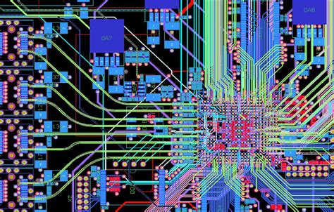
Introduction to PCB Transmission Lines
Printed Circuit Boards (PCBs) are essential components in modern electronics, providing a platform for interconnecting various electronic components. As the operating frequencies of these components continue to increase, the design of PCBs becomes more complex, requiring a thorough understanding of high-speed signal propagation. One critical aspect of high-speed PCB design is the concept of transmission lines.
What are Transmission Lines?
Transmission lines are structures designed to efficiently transfer electromagnetic energy from one point to another. In the context of PCBs, transmission lines are used to carry high-speed signals between components while minimizing signal distortion and maintaining signal integrity.
Importance of Transmission Line Principles in PCB Design
Understanding transmission line principles is crucial for successful high-speed PCB design. Improper design of transmission lines can lead to signal integrity issues, such as:
- Signal reflections
- Crosstalk
- Electromagnetic interference (EMI)
- Signal attenuation
- Timing errors
By applying transmission line principles, PCB designers can mitigate these issues and ensure reliable communication between components.
Fundamental Concepts of Transmission Lines
Characteristic Impedance
Characteristic impedance is a key parameter of transmission lines. It is the ratio of the voltage to the current in a transmission line when the line is infinitely long or perfectly matched. The characteristic impedance is determined by the physical properties of the transmission line, such as its geometry, dielectric constant, and conductor material.
The characteristic impedance of a transmission line is given by:
Z0 = sqrt(L/C)
Where:
– Z0 is the characteristic impedance
– L is the inductance per unit length
– C is the capacitance per unit length
Matching the characteristic impedance of the transmission line to the impedance of the source and load is essential for minimizing signal reflections and ensuring optimal power transfer.
Propagation Velocity
Propagation velocity, also known as phase velocity, is the speed at which an electromagnetic wave travels along a transmission line. It is determined by the dielectric constant of the PCB material and the speed of light in a vacuum.
The propagation velocity of a transmission line is given by:
v = c / sqrt(εr)
Where:
– v is the propagation velocity
– c is the speed of light in a vacuum (approximately 3 × 10^8 m/s)
– εr is the relative dielectric constant of the PCB material
Understanding the propagation velocity is important for calculating signal delays and ensuring proper timing of signals across the PCB.
Reflection Coefficient
The reflection coefficient is a measure of the amount of signal reflection that occurs when a transmission line is not perfectly matched to its load. It is defined as the ratio of the reflected voltage to the incident voltage.
The reflection coefficient is given by:
Γ = (ZL - Z0) / (ZL + Z0)
Where:
– Γ (Gamma) is the reflection coefficient
– ZL is the load impedance
– Z0 is the characteristic impedance of the transmission line
A reflection coefficient of zero indicates a perfectly matched transmission line, while a reflection coefficient of ±1 indicates a complete reflection of the signal.
Types of Transmission Lines in PCBs
Microstrip Lines
Microstrip lines are the most common type of transmission line used in PCBs. They consist of a single conductor trace on the top layer of the PCB, with a ground plane on the bottom layer. The characteristic impedance of a microstrip line is determined by the width of the trace, the thickness of the dielectric material, and the dielectric constant of the PCB material.
| Parameter | Symbol | Description |
|---|---|---|
| Trace Width | W | Width of the microstrip trace |
| Dielectric Thickness | H | Thickness of the dielectric material between the trace and ground plane |
| Dielectric Constant | εr | Relative permittivity of the PCB material |
The characteristic impedance of a microstrip line can be approximated using the following equations:
For W/H ≤ 1:
Z0 = (87 / sqrt(εr + 1.41)) * ln(5.98 * H / (0.8 * W + T))
For W/H > 1:
Z0 = (120π / sqrt(εr)) / (W/H + 1.393 + 0.667 * ln(W/H + 1.444))
Where:
– T is the thickness of the microstrip trace
Stripline
Striplines are another type of transmission line used in PCBs. They consist of a single conductor trace embedded between two ground planes. Striplines offer better shielding and lower radiation compared to microstrip lines, making them suitable for sensitive or high-speed applications.
The characteristic impedance of a stripline is determined by the width of the trace, the distance between the ground planes, and the dielectric constant of the PCB material.
| Parameter | Symbol | Description |
|---|---|---|
| Trace Width | W | Width of the stripline trace |
| Dielectric Thickness | H | Distance between the two ground planes |
| Dielectric Constant | εr | Relative permittivity of the PCB material |
The characteristic impedance of a stripline can be approximated using the following equation:
Z0 = (60 / sqrt(εr)) * ln(4 * H / (0.67 * (0.8 * W + T)))
Where:
– T is the thickness of the stripline trace
Coplanar Waveguide
Coplanar waveguides (CPWs) are transmission lines that consist of a single conductor trace with ground planes on either side, all on the same layer of the PCB. CPWs offer low dispersion and are suitable for high-frequency applications.
The characteristic impedance of a CPW is determined by the width of the trace, the gap between the trace and the ground planes, and the dielectric constant of the PCB material.
| Parameter | Symbol | Description |
|---|---|---|
| Trace Width | W | Width of the CPW trace |
| Gap Width | G | Width of the gap between the trace and ground planes |
| Dielectric Constant | εr | Relative permittivity of the PCB material |
The characteristic impedance of a CPW can be approximated using the following equation:
Z0 = (30π / sqrt(εr)) * (K(k') / K(k))
Where:
– K(k) and K(k’) are complete elliptic integrals of the first kind
– k = W / (W + 2G)
– k’ = sqrt(1 – k^2)

PCB Transmission Line Design Considerations
Impedance Matching
Impedance matching is essential for minimizing signal reflections and ensuring optimal power transfer in PCB transmission lines. To achieve impedance matching, the characteristic impedance of the transmission line must be matched to the impedance of the source and load.
Common impedance values used in PCB design include:
- 50 ohms: Commonly used in RF and high-speed digital applications
- 75 ohms: Used in video and cable TV applications
- 100 ohms: Used in Ethernet and other balanced transmission lines
Impedance matching can be achieved through proper selection of PCB material, trace geometry, and termination techniques.
Termination Techniques
Termination techniques are used to minimize signal reflections and ensure proper impedance matching in PCB transmission lines. Some common termination techniques include:
- Series termination: A resistor is placed in series with the source to match the characteristic impedance of the transmission line.
- Parallel termination: A resistor is placed in parallel with the load to match the characteristic impedance of the transmission line.
- AC termination: A combination of resistors and capacitors is used to provide frequency-dependent termination.
- Differential termination: Used in differential signaling schemes to match the differential impedance of the transmission line.
The choice of termination technique depends on factors such as the signal frequency, the length of the transmission line, and the impedance of the source and load.
Length Matching
Length matching is the process of ensuring that the electrical lengths of transmission lines are equal to maintain proper timing and phase relationships between signals. This is particularly important in high-speed digital systems where multiple signals must arrive at their destinations simultaneously.
Length matching can be achieved through careful routing of transmission lines, using meandering traces, or by adding delay elements such as serpentine traces or programmable delay lines.
Crosstalk Reduction
Crosstalk is the unintended coupling of signals between adjacent transmission lines, which can lead to signal integrity issues. To reduce crosstalk, PCB designers can:
- Increase the spacing between transmission lines
- Use guard traces or ground planes between sensitive signals
- Route sensitive signals on different layers of the PCB
- Use differential signaling techniques
By minimizing crosstalk, designers can ensure that signals maintain their integrity and avoid interference from neighboring traces.
Simulation and Modeling of PCB Transmission Lines
SPICE Modeling
SPICE (Simulation Program with Integrated Circuit Emphasis) is a widely used tool for simulating and modeling electronic circuits, including PCB transmission lines. SPICE models can be used to analyze the behavior of transmission lines, including impedance, propagation delay, and signal integrity.
To create a SPICE model of a PCB transmission line, designers need to specify the physical properties of the transmission line, such as its length, width, thickness, and dielectric constant. The model can then be used to simulate the response of the transmission line to various input signals and load conditions.
Electromagnetic Simulation
Electromagnetic simulation tools, such as finite element analysis (FEA) and method of moments (MoM), can be used to model the electromagnetic behavior of PCB transmission lines. These tools can provide detailed information about the electric and magnetic fields surrounding the transmission line, as well as the effects of dielectric materials and conductor losses.
Electromagnetic simulation is particularly useful for analyzing complex PCB structures, such as vias, bends, and discontinuities, which can have a significant impact on signal integrity.
Frequently Asked Questions (FAQ)
-
What is the difference between a microstrip and a stripline?
A microstrip is a transmission line with a single conductor trace on the top layer of the PCB, above a ground plane. In contrast, a stripline is a transmission line with a single conductor trace embedded between two ground planes. Striplines offer better shielding and lower radiation compared to microstrips. -
What is the purpose of impedance matching in PCB transmission lines?
Impedance matching is used to minimize signal reflections and ensure optimal power transfer in PCB transmission lines. By matching the characteristic impedance of the transmission line to the impedance of the source and load, designers can reduce signal distortion and maintain signal integrity. -
How can I reduce crosstalk between transmission lines on a PCB?
To reduce crosstalk between transmission lines, designers can increase the spacing between traces, use guard traces or ground planes between sensitive signals, route sensitive signals on different layers of the PCB, or employ differential signaling techniques. -
What is the role of SPICE modeling in PCB transmission line design?
SPICE modeling is used to simulate and analyze the behavior of PCB transmission lines, including impedance, propagation delay, and signal integrity. By creating a SPICE model of a transmission line, designers can predict its response to various input signals and load conditions, helping to optimize the design. -
Why is length matching important in high-speed digital systems?
Length matching is crucial in high-speed digital systems to ensure that multiple signals arrive at their destinations simultaneously. By matching the electrical lengths of transmission lines, designers can maintain proper timing and phase relationships between signals, reducing signal integrity issues and ensuring reliable system operation.
Conclusion
PCB transmission line principles play a critical role in the design of high-speed electronic systems. By understanding the fundamental concepts of transmission lines, such as characteristic impedance, propagation velocity, and reflection coefficient, PCB designers can create robust and reliable interconnects that maintain signal integrity.
Proper design of transmission lines involves selecting the appropriate type of transmission line, such as microstrip, stripline, or coplanar waveguide, and applying techniques like impedance matching, termination, length matching, and crosstalk reduction. Simulation and modeling tools, such as SPICE and electromagnetic simulation, can further aid in the analysis and optimization of PCB transmission line designs.
As electronic systems continue to push the boundaries of speed and complexity, mastering PCB transmission line principles becomes increasingly important for engineers and designers. By applying these principles effectively, they can create high-performance PCBs that enable the next generation of innovative electronic products.

No responses yet