What are IC Substrates?
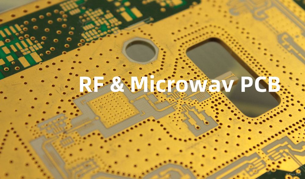
IC substrates, also known as chip carriers or package substrates, are advanced PCBs that serve as the interface between an integrated circuit (IC) chip and the larger PCB or electronic device. These substrates are designed to provide electrical connections, mechanical support, and thermal management for the IC chip.
Key Features of IC Substrates
- High-Density Interconnects (HDI): IC substrates feature fine-pitch traces and vias, enabling the connection of a large number of input/output (I/O) points on the IC chip to the substrate.
- Multi-Layer Construction: IC substrates often consist of multiple layers of conductive traces and dielectric materials, allowing for complex routing and signal integrity.
- Thermal Management: The substrate material and design help dissipate heat generated by the IC chip, ensuring optimal performance and reliability.
- Compatibility with Various Packaging Technologies: IC substrates are compatible with different IC packaging technologies, such as flip-chip, wire bonding, and ball grid array (BGA).
IC Substrate Manufacturing Process
The manufacturing process of IC substrates involves several critical steps to ensure high precision and reliability:
- Material Selection: The choice of substrate material depends on the specific requirements of the IC package, such as electrical properties, thermal conductivity, and mechanical strength. Common materials include bismaleimide triazine (BT), glass-reinforced epoxy (FR-4), and polyimide.
- Patterning: The conductive traces and vias are patterned onto the substrate using photolithography and etching processes. Advanced techniques like semi-additive process (SAP) and modified semi-additive process (mSAP) enable the creation of fine-pitch features.
- Lamination: Multiple layers of patterned substrates are laminated together using heat and pressure to form a multi-layer structure.
- Surface Finishing: The exposed copper traces are plated with a protective layer, such as nickel/gold (ENIG) or organic solderability preservative (OSP), to prevent oxidation and enhance solderability.
- Singulation: The panel containing multiple IC substrates is cut into individual units using precise dicing or laser cutting techniques.
| Step | Process | Description |
|---|---|---|
| 1 | Material Selection | Choose substrate material based on requirements |
| 2 | Patterning | Create conductive traces and vias using photolithography and etching |
| 3 | Lamination | Laminate multiple patterned layers together |
| 4 | Surface Finishing | Plate exposed copper traces with protective layer |
| 5 | Singulation | Cut panel into individual IC substrates |
What are IC Probe Cards?
IC probe cards are specialized PCBs used in the wafer-level testing of integrated circuits. These cards interface with the IC wafer and provide electrical connections between the test equipment and the individual IC dies on the wafer. Probe cards play a critical role in ensuring the functionality and performance of ICs before they are packaged.
Key Features of IC Probe Cards
- High Pin Count: Probe cards can accommodate a large number of probes, enabling simultaneous testing of multiple IC dies on a wafer.
- Precise Probe Alignment: The probes on the card must align accurately with the contact pads on the IC dies to establish reliable electrical connections.
- Signal Integrity: Probe cards are designed to maintain signal integrity during high-frequency testing, minimizing cross-talk and signal distortion.
- Mechanical Stability: The probe card assembly must withstand repeated contact cycles while maintaining consistent probe alignment and contact force.
IC Probe Card Manufacturing Process
The manufacturing process of IC probe cards involves precision engineering and assembly techniques:
- PCB fabrication: The probe card PCB is fabricated using advanced PCB manufacturing processes, similar to those used for IC substrates.
- Probe Assembly: The probes, typically made of tungsten or beryllium-copper alloy, are precisely aligned and attached to the probe card PCB using epoxy or solder.
- Planarization: The probe tips are planarized to ensure uniform contact with the IC wafer surface.
- Probe Card Testing: The assembled probe card undergoes rigorous testing to verify probe alignment, electrical continuity, and signal integrity.
| Step | Process | Description |
|---|---|---|
| 1 | PCB Fabrication | Fabricate probe card PCB using advanced manufacturing processes |
| 2 | Probe Assembly | Align and attach probes to the probe card PCB |
| 3 | Planarization | Planarize probe tips for uniform contact with IC wafer |
| 4 | Probe Card Testing | Test assembled probe card for alignment, continuity, and signal integrity |
Advancements in IC PCBs
The increasing complexity and miniaturization of integrated circuits have driven advancements in IC substrate and probe card technologies. Some notable developments include:
- 2.5D and 3D IC Packaging: IC substrates have evolved to support 2.5D and 3D packaging technologies, where multiple IC chips are stacked or interconnected using through-silicon vias (TSVs) and silicon interposers.
- Fine-Pitch Probe Cards: Probe cards with pitch sizes below 40 μm have been developed to accommodate the shrinking geometries of advanced IC nodes.
- MEMS Probe Cards: Micro-Electro-Mechanical Systems (MEMS) technology has been applied to probe cards, enabling high probe density, improved contact reliability, and reduced probe wear.
- Active Probe Cards: Active probe cards incorporate active electronic components, such as amplifiers and switches, directly on the probe card to enhance signal integrity and enable advanced testing capabilities.

Challenges and Future Trends
As the electronics industry continues to push the boundaries of IC performance and integration, IC substrates and probe cards face several challenges and opportunities:
- Increasing I/O Density: The demand for higher I/O counts and finer pitch sizes in IC packages requires advancements in substrate manufacturing processes and materials.
- Signal Integrity: Maintaining signal integrity becomes more challenging as data rates increase and signal frequencies rise. Innovations in substrate design, materials, and simulation tools are necessary to address these challenges.
- Cost Reduction: The cost of IC substrates and probe cards contributes significantly to the overall cost of IC packaging and testing. Efforts to optimize manufacturing processes, materials, and design for cost-effectiveness are ongoing.
- Heterogeneous Integration: The trend towards heterogeneous integration, combining multiple types of ICs and components in a single package, requires versatile and adaptable IC substrate solutions.
- Wafer-Level Packaging: The adoption of wafer-level packaging (WLP) techniques, where ICs are packaged directly on the wafer, necessitates the development of specialized probe cards compatible with WLP processes.
Frequently Asked Questions (FAQ)
1. What is the difference between an IC substrate and a regular PCB?
An IC substrate is a specialized PCB Designed to interface with an integrated circuit (IC) chip. It features high-density interconnects, fine-pitch traces, and multi-layer construction to accommodate the large number of I/O points on the IC chip. In contrast, a regular PCB is used to interconnect various electronic components and typically has larger feature sizes and lower connection densities.
2. Why are IC probe cards important in the IC manufacturing process?
IC probe cards are essential for wafer-level testing of integrated circuits before they are packaged. They provide electrical connections between the test equipment and the individual IC dies on the wafer, enabling functional and performance testing. Probe cards ensure that only known good dies (KGDs) are packaged, reducing waste and improving yield.
3. What materials are commonly used for IC substrates?
Common materials used for IC substrates include:
– Bismaleimide triazine (BT): A high-performance thermoset polymer with good electrical and mechanical properties.
– Glass-reinforced epoxy (FR-4): A widely used PCB material offering a balance of cost, performance, and processability.
– Polyimide: A high-temperature resistant polymer with excellent electrical and mechanical properties.
The choice of material depends on the specific requirements of the IC package, such as electrical performance, thermal management, and reliability.
4. How do IC probe cards maintain precise probe alignment with the IC wafer?
IC probe cards employ precise mechanical alignment techniques to ensure accurate probe placement on the IC wafer. This is achieved through:
– Precise PCB fabrication: The probe card PCB is manufactured with tight tolerances to maintain accurate probe positions.
– Probe assembly: The probes are carefully aligned and attached to the probe card PCB using specialized equipment and techniques, such as vision systems and micro-positioners.
– Planarization: The probe tips are planarized to ensure uniform contact with the IC wafer surface, compensating for any minor variations in probe height.
Regular maintenance and calibration of the probe card are also essential to maintain alignment accuracy over multiple contact cycles.
5. What are the challenges in designing and manufacturing IC substrates for high-frequency applications?
Designing and manufacturing IC substrates for high-frequency applications pose several challenges:
– Signal integrity: High-frequency signals are susceptible to signal degradation, cross-talk, and reflections. Careful design and simulation are required to optimize trace routing, Impedance Matching, and shielding.
– Material selection: The choice of substrate material is critical for high-frequency performance. Low-loss dielectrics and high-conductivity metals are necessary to minimize signal attenuation and distortion.
– Manufacturing processes: Advanced manufacturing techniques, such as semi-additive process (SAP) and modified semi-additive process (mSAP), are needed to achieve fine-pitch traces and tight tolerances required for high-frequency substrates.
– Testing and characterization: Comprehensive testing and characterization of the substrate’s electrical properties, such as insertion loss, return loss, and cross-talk, are essential to ensure performance in the target frequency range.
Collaboration between IC designers, substrate manufacturers, and packaging engineers is crucial to overcome these challenges and develop high-performance IC substrates for high-frequency applications.
Conclusion
IC substrates and IC probe cards are highly advanced and specialized PCBs that play a vital role in the packaging and testing of integrated circuits. These PCBs feature high-density interconnects, fine-pitch traces, and multi-layer construction to accommodate the increasing complexity and miniaturization of ICs.
The manufacturing processes for IC substrates and probe cards involve precise patterning, lamination, assembly, and testing techniques to ensure reliable electrical connections and signal integrity. Advancements in materials, design, and manufacturing technologies continue to push the boundaries of IC packaging and testing capabilities.
As the demand for higher performance, integration, and functionality in electronic devices grows, IC substrates and probe cards will remain critical components in the electronics industry. Ongoing research and development efforts aim to address challenges related to signal integrity, cost reduction, heterogeneous integration, and wafer-level packaging.
By understanding the intricacies of IC substrates and IC probe cards, electronics manufacturers, designers, and engineers can leverage these advanced PCB technologies to create innovative and reliable electronic products that meet the ever-evolving needs of consumers and industries alike.

No responses yet