Understanding High-Frequency Signals
To grasp the significance of High-Frequency PCBs, it is essential to understand high-frequency signals. High-frequency signals are electrical signals that oscillate at a high rate, typically in the range of megahertz (MHz) to gigahertz (GHz). These signals are used in various applications, including:
- Wireless communication systems (e.g., cellular networks, Wi-Fi, Bluetooth)
- Radar and satellite systems
- High-speed digital circuits (e.g., computer processors, memory interfaces)
- RF and microwave circuits (e.g., amplifiers, filters, antennas)
High-frequency signals behave differently compared to low-frequency signals. They are more susceptible to signal integrity issues, such as signal distortion, attenuation, and interference. Therefore, designing and manufacturing PCBs that can effectively handle high-frequency signals requires special considerations and techniques.
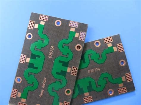
Structure of High-Frequency PCBs
High-frequency PCBs have a specific structure that enables them to handle high-frequency signals effectively. The key components of a high-frequency PCB structure include:
Substrate Material
The substrate material is the foundation of a PCB, providing mechanical support and electrical insulation. For high-frequency PCBs, the choice of substrate material is crucial. Common substrate materials used in high-frequency PCBs include:
- FR-4: A popular and cost-effective substrate material for general-purpose PCBs. However, its performance degrades at higher frequencies.
- Rogers materials (e.g., RO4003, RO4350B): High-performance substrate materials specifically designed for high-frequency applications. They offer excellent electrical properties, such as low dielectric loss and stable dielectric constant.
- PTFE (Polytetrafluoroethylene): Another high-performance substrate material known for its low dielectric loss and stable dielectric constant.
The choice of substrate material depends on the specific requirements of the application, such as the operating frequency, signal integrity, and cost considerations.
Copper Traces
Copper traces are the conductive paths that carry electrical signals on a PCB. In high-frequency PCBs, the design and layout of copper traces are critical for maintaining signal integrity. Some key considerations for copper traces in high-frequency PCBs include:
- Trace width and thickness: The width and thickness of copper traces affect their impedance and current-carrying capacity. Proper trace dimensions are crucial for impedance matching and minimizing signal reflections.
- Trace routing: The routing of copper traces should be optimized to minimize signal distortion and crosstalk. Techniques such as microstrip, stripline, and coplanar waveguide (CPW) are commonly used for high-frequency trace routing.
- Trace length matching: In high-speed digital circuits, trace length matching is essential to ensure synchronized signal arrival at the receiver. Techniques such as serpentine routing and delay lines are used to achieve trace length matching.
Ground and Power Planes
Ground and power planes play a vital role in high-frequency PCBs. They provide a low-impedance return path for high-frequency signals and help in shielding and noise reduction. Some key considerations for ground and power planes in high-frequency PCBs include:
- Solid planes: Using solid ground and power planes helps in reducing impedance and providing better shielding compared to gridded or hatched planes.
- Plane spacing: The spacing between the ground and power planes affects the impedance and capacitance of the PCB. Proper spacing is necessary to achieve the desired impedance and minimize noise coupling.
- Via placement: The placement of vias connecting the ground and power planes to the signal layers should be carefully considered to minimize signal distortion and ensure proper grounding.
Multilayer Stackup
High-frequency PCBs often employ a multilayer stackup to accommodate complex circuitry and provide better signal integrity. A typical high-frequency PCB stackup may include:
- Signal layers: Layers dedicated to routing high-frequency signals.
- Ground and power planes: Layers dedicated to providing a low-impedance return path and power distribution.
- Dielectric layers: Insulating layers separating the signal layers and ground/power planes.
The arrangement of layers in the stackup depends on the specific application and the desired electrical performance. Proper layer arrangement helps in minimizing crosstalk, reducing electromagnetic interference (EMI), and improving signal integrity.

Types of High-Frequency PCBs
High-frequency PCBs can be classified into different types based on their construction and application. Some common types of high-frequency PCBs include:
Microwave PCBs
Microwave PCBs are designed to handle signals in the microwave frequency range, typically from 1 GHz to 30 GHz. These PCBs are used in applications such as radar systems, satellite communication, and wireless base stations. Microwave PCBs require specialized substrate materials, such as PTFE or Rogers materials, to minimize dielectric loss and ensure stable performance at high frequencies.
RF PCBs
RF PCBs are designed to handle signals in the radio frequency range, typically from a few MHz to several GHz. These PCBs are used in applications such as wireless communication devices, RF amplifiers, and RF filters. RF PCBs require careful design considerations, such as impedance matching, trace routing, and shielding, to ensure optimal signal integrity and minimize interference.
High-Speed Digital PCBs
High-speed digital PCBs are designed to handle high-speed digital signals, such as those found in computer processors, memory interfaces, and high-speed data communication systems. These PCBs require precise trace routing, impedance control, and signal integrity management to ensure reliable data transmission at high speeds.
Hybrid PCBs
Hybrid PCBs combine different types of high-frequency circuits on a single board. For example, a hybrid PCB may include both RF and high-speed digital circuits. Hybrid PCBs require careful design considerations to ensure proper isolation and compatibility between the different circuit types.

Key Considerations in High-Frequency PCB Design
Designing high-frequency PCBs involves several key considerations to ensure optimal performance and signal integrity. Some of these considerations include:
Impedance Matching
Impedance matching is crucial in high-frequency PCB design to minimize signal reflections and ensure maximum power transfer. The characteristic impedance of the transmission lines (traces) should match the impedance of the source and load. Common impedance values used in high-frequency PCBs include 50 ohms and 75 ohms.
Signal Integrity
Signal integrity refers to the quality and fidelity of the signals propagating through the PCB. In high-frequency PCBs, signal integrity is affected by various factors, such as impedance mismatch, crosstalk, signal attenuation, and reflections. Proper PCB design techniques, such as Controlled Impedance routing, differential signaling, and shielding, help in maintaining signal integrity.
Electromagnetic Compatibility (EMC)
EMC refers to the ability of electronic devices to operate without causing or being affected by electromagnetic interference (EMI). High-frequency PCBs are susceptible to EMI due to the nature of high-frequency signals. Proper EMC design practices, such as shielding, grounding, and filtering, are essential to ensure the PCB meets EMC regulations and operates reliably in its intended environment.
Thermal Management
High-frequency PCBs often generate significant heat due to the high power dissipation of the components and the high-frequency operation. Proper thermal management is crucial to ensure the reliability and performance of the PCB. Techniques such as using Thermal Vias, heat sinks, and proper component placement help in dissipating heat effectively.
Manufacturing Considerations
Manufacturing high-frequency PCBs requires specialized processes and expertise. Some key manufacturing considerations include:
- Material selection: Choosing the appropriate substrate material and copper foil thickness based on the application requirements.
- Fabrication processes: Using advanced fabrication techniques, such as high-density interconnect (HDI), microvias, and controlled depth drilling, to achieve precise and reliable high-frequency PCBs.
- Lamination and bonding: Ensuring proper lamination and bonding of the layers to maintain the desired electrical properties and prevent delamination.
- Testing and inspection: Performing rigorous testing and inspection procedures to verify the electrical performance, signal integrity, and reliability of the manufactured PCBs.

Frequently Asked Questions (FAQ)
1. What is the difference between high-frequency PCBs and regular PCBs?
High-frequency PCBs are specifically designed to handle high-frequency signals, typically in the range of MHz to GHz. They require specialized substrate materials, precise trace routing, and careful consideration of signal integrity and EMC. Regular PCBs, on the other hand, are designed for lower frequency applications and may not have the same level of performance and design considerations as high-frequency PCBs.
2. What are the common applications of high-frequency PCBs?
High-frequency PCBs are used in various applications that involve high-frequency signals, such as:
– Wireless communication devices (e.g., cellular phones, Wi-Fi routers, Bluetooth devices)
– Radar and satellite systems
– High-speed digital circuits (e.g., computer processors, memory interfaces)
– RF and microwave circuits (e.g., amplifiers, filters, antennas)
– Medical imaging systems (e.g., MRI, ultrasound)
– Automotive electronics (e.g., radar sensors, infotainment systems)
3. What is the role of substrate material in high-frequency PCBs?
The substrate material is a critical component in high-frequency PCBs. It provides the foundation for the PCB and affects its electrical properties. The choice of substrate material depends on the specific application and the desired performance characteristics. Common substrate materials used in high-frequency PCBs include FR-4, Rogers materials (e.g., RO4003, RO4350B), and PTFE. These materials offer different levels of dielectric constant, dielectric loss, and thermal stability, which are important factors in high-frequency PCB design.
4. What are the challenges in designing high-frequency PCBs?
Designing high-frequency PCBs presents several challenges, including:
– Maintaining signal integrity: High-frequency signals are susceptible to distortion, attenuation, and interference. Proper trace routing, impedance matching, and shielding techniques are essential to maintain signal integrity.
– Controlling EMI: High-frequency PCBs can generate and be affected by electromagnetic interference (EMI). Proper EMC design practices, such as shielding, grounding, and filtering, are necessary to mitigate EMI issues.
– Thermal management: High-frequency PCBs often generate significant heat, which can affect the performance and reliability of the components. Effective thermal management techniques, such as using thermal vias and heat sinks, are crucial.
– Manufacturing complexity: Manufacturing high-frequency PCBs requires specialized processes and expertise. Challenges include precise material selection, advanced fabrication techniques, and rigorous testing and inspection procedures.
5. How can signal integrity be ensured in high-frequency PCBs?
Ensuring signal integrity in high-frequency PCBs involves several techniques, including:
– Impedance matching: Matching the characteristic impedance of the traces to the impedance of the source and load to minimize signal reflections and ensure maximum power transfer.
– Controlled impedance routing: Using techniques such as microstrip, stripline, and coplanar waveguide (CPW) to achieve controlled impedance and minimize signal distortion.
– Differential signaling: Using differential pairs to transmit signals, which helps in canceling out common-mode noise and improving signal integrity.
– Shielding: Employing shielding techniques, such as ground planes and shielding enclosures, to reduce crosstalk and EMI.
– Proper grounding: Implementing a robust grounding strategy to provide a low-impedance return path for high-frequency signals and minimize ground bounce.
– Trace length matching: Ensuring equal trace lengths for critical signals to maintain synchronization and prevent timing issues.
Conclusion
High-frequency PCBs are essential components in various electronic devices and systems that operate at high frequencies. Understanding the structure, types, and key considerations in high-frequency PCB design is crucial for engineers and manufacturers working in this field. By carefully selecting substrate materials, designing precise trace routing, and implementing proper signal integrity and EMC techniques, high-frequency PCBs can be designed and manufactured to meet the demanding requirements of modern electronic applications.
As technology continues to advance and the demand for high-frequency electronics grows, the importance of high-frequency PCBs will only increase. Staying up-to-date with the latest design techniques, materials, and manufacturing processes is essential for engineers and manufacturers to stay competitive in this evolving field.
| Parameter | Description |
|---|---|
| Frequency Range | The range of frequencies that the high-frequency PCB is designed to handle, typically in the range of MHz to GHz. |
| Substrate Material | The foundation material of the PCB, such as FR-4, Rogers materials, or PTFE, which affects the electrical properties and performance of the PCB. |
| Dielectric Constant | A measure of the substrate material’s ability to store electrical energy, which affects the signal propagation and impedance of the PCB. |
| Dielectric Loss | A measure of the energy dissipation in the substrate material, which affects the signal attenuation and quality at high frequencies. |
| Copper Thickness | The thickness of the copper foil used for the conductive traces on the PCB, which affects the current-carrying capacity and impedance of the traces. |
| Trace Width | The width of the conductive traces on the PCB, which affects the impedance and signal integrity of the high-frequency signals. |
| Impedance | The opposition to the flow of high-frequency signals in the PCB, which should be matched to the impedance of the source and load for optimal signal transfer. |
| Multilayer Stackup | The arrangement of multiple layers in the PCB, including signal layers, ground and power planes, and dielectric layers, which affects the signal integrity and EMC performance. |
By carefully considering and optimizing these parameters, engineers can design high-frequency PCBs that meet the specific requirements of their applications and ensure reliable performance in the high-frequency domain.
No responses yet