What is Reflow Soldering?
Reflow soldering is a technique where solder paste (a mixture of tiny solder spheres and flux) is applied to the conductive pads on a PCB. Surface mount components are then placed onto the solder paste. The populated PCB is sent through a reflow oven, which heats up the board to specific temperatures in zones to activate the flux, melt the solder, and form reliable solder joints between the component leads and pads. Reflow soldering enables the fast, automated assembly of high-density electronic circuits.
Advantages of Reflow Soldering
- Fast and efficient for high-volume production
- Precise and repeatable solder joint quality
- Handles high component density and small pitches
- Suitable for single- and double-sided PCB Assembly
- Easily automated with pick-and-place machines and conveyor ovens
Equipment and Materials Needed
To get started with reflow soldering, you will need the following:
- Solder Paste
- No-clean, lead-free solder paste (e.g., SAC305)
- Comes in jars or syringes for dispensing
- Stencil
- Laser-cut or electroformed stencil with apertures matching PCB pads
- Used to apply solder paste to the PCB
- Squeegees/Solder Paste Applicators
- Metal or plastic blades for spreading solder paste through the stencil
- Pick-and-Place Machine (Optional)
- Automated system for placing components on the PCB
- Essential for high-volume production
- Tweezers
- For manual component placement and adjustments
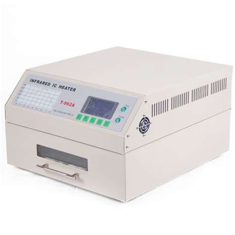
- Reflow Oven
- Tabletop or conveyor oven with multiple heating zones
- Follows a specific temperature profile to melt the solder
- PCB Preheater (Optional)
- Separate preheating stage to gradually warm up the PCB
- Helps prevent thermal shock and improves joint quality
- Fume Extractor
- Removes solder flux fumes generated during reflow
- Cleaning Supplies
- Isopropyl alcohol, brushes, and wipes for post-reflow cleaning

Reflow Soldering Process Steps
Step 1: PCB Preparation
- Design the PCB layout with appropriate pad sizes and solder mask openings for the components used.
- Ensure the PCB surface is clean and free of contaminants like dirt, grease, or oxidation.
- If needed, apply a thin layer of liquid flux to the pads to enhance solderability.
Step 2: Solder Paste Application
- Place the solder paste stencil on top of the PCB, aligning it with the pads and fiducials.
- Dispense an appropriate amount of solder paste at one end of the stencil.
- Use a squeegee blade to spread the paste across the stencil, filling the apertures.
- Lift the stencil vertically to leave precise deposits of solder paste on each pad.
- Inspect the pasted PCB for any defects like bridging, insufficient paste, or misalignment.
Step 3: Component Placement
- Using tweezers or a pick-and-place machine, carefully place each component onto its corresponding pads.
- Ensure the component leads are centered on the solder paste deposits.
- For small or fine-pitch components, use magnification and take precautions against static discharge.
- Inspect the populated board for proper Component Orientation, alignment, and absence of damage.
Step 4: Reflow Soldering
- Preheat the populated PCB (if using a separate preheater) to around 150°C to activate the flux and start evaporating solvents.
- Transfer the board to the reflow oven, which will heat it according to a specific temperature profile.
- The reflow profile typically consists of four stages:
- Preheat: Gradual ramp up to 150-180°C to activate flux and evaporate solvents
- Thermal Soak: Holding at a stable temperature to equalize board temperature
- Reflow: Quick ramp up to 240-250°C to melt the solder and form interconnects
- Cooling: Gradual cool down to solidify the solder joints
- Exact temperatures and durations depend on the solder paste, board size, and component density.
- Monitor the oven temperature and belt speed to ensure the profile is followed correctly.
Step 5: Inspection and Cleaning
- After cooling, visually inspect the reflowed board for solder joint quality and defects.
- Use a microscope to check for bridging, insufficient solder, tombstoning, or lifted components.
- If applicable, perform electrical testing to verify proper connections and circuit function.
- Clean flux residues from the board using isopropyl alcohol, brushes, or specialized cleaners.
- Apply conformal coating if required for environmental protection.

Reflow Soldering Temperature Profile
The reflow temperature profile is critical for achieving good solder joints and preventing component damage. It specifies the temperatures and durations for each stage of the reflow process. Here’s a sample lead-free reflow profile:
| Stage | Temperature Range | Duration |
|---|---|---|
| Preheat | 25°C to 150°C | 60-90 sec |
| Soak | 150°C to 180°C | 60-120 sec |
| Reflow | 240°C to 250°C | 30-60 sec |
| Cooling | 250°C to 25°C | 30-90 sec |
Factors influencing the optimal reflow profile include:
– Solder paste composition and melting point
– PCB Thickness, size, and thermal mass
– Component density and heat sensitivity
– Oven type and heating method
Consult the solder paste and component datasheets for specific recommendations. Use thermocouples and profiling software to monitor and adjust the actual temperature profile.

Troubleshooting Common Reflow Soldering Defects
Despite careful process control, reflow soldering can occasionally result in defects that affect circuit reliability. Here are some common issues and their potential causes:
| Defect | Description | Possible Causes |
|---|---|---|
| Bridging | Solder connecting adjacent pads or leads | Excess solder paste, poor stencil design |
| Insufficient | Not enough solder, weak or cracked joints | Too little paste, poor wetting |
| Tombstoning | One end of component lifts up vertically | Uneven heating, misaligned pads |
| Solder Balls | Small spheres of solder stuck to pads or mask | Contamination, excess flux |
| Poor Wetting | Solder not adhering or spreading on pads | Oxide on pads, insufficient flux |
| Lifted Components | Components detached from pads after reflow | Thermal mismatch, mechanical stress |
| Flux Residue | Sticky or discolored residue on board surface | Incorrect profile, non-cleanable flux |
To minimize defects, ensure proper PCB design, maintain paste and stencil quality, optimize placement accuracy, follow recommended profiles, and control environment conditions.
Frequently Asked Questions
What is the difference between reflow and Wave Soldering?
Reflow soldering is used for surface mount components, where solder paste is applied to pads, components are placed, and the assembly is heated to melt the solder. Wave soldering is used for through-hole components, where the board is passed over a molten solder wave to fill the holes and create joints.
Can I reflow solder without a stencil?
While stencils are recommended for precise, repeatable solder paste application, it is possible to manually apply paste using syringes or dispensing needles. This is more time-consuming and less consistent, suitable only for small batches or repairs.
How long does solder paste last?
Solder paste has a limited shelf life, typically around 6 months when refrigerated. Unopened paste can last up to a year. Once opened, the paste should be used within a few days to avoid drying out or oxidation. Always check the manufacturer’s storage and handling guidelines.
Can I reuse solder paste?
Leftover solder paste from a previous job should not be reused, as it may have started to dry out or been contaminated. Dispose of any unused paste properly and use fresh paste for each new assembly.
How do I select the right solder paste?
The main factors in choosing a solder paste are the alloy composition (e.g., lead-free SAC305), particle size (T3-T5 for standard pitches), and flux type (no-clean, water-soluble, rosin). Match the paste properties to your PCB design, components, and reflow profile. Consult with paste suppliers for specific recommendations.
Conclusion
Reflow soldering is a versatile and efficient method for assembling surface mount PCBs. By understanding the process steps, equipment, and best practices, you can achieve high-quality solder joints and reliable circuits. Proper paste selection, stencil design, component placement, and temperature profiling are key to success. With practice and attention to detail, reflow soldering can enable the production of complex, high-performance electronic assemblies.
No responses yet