Introduction to PCB Design
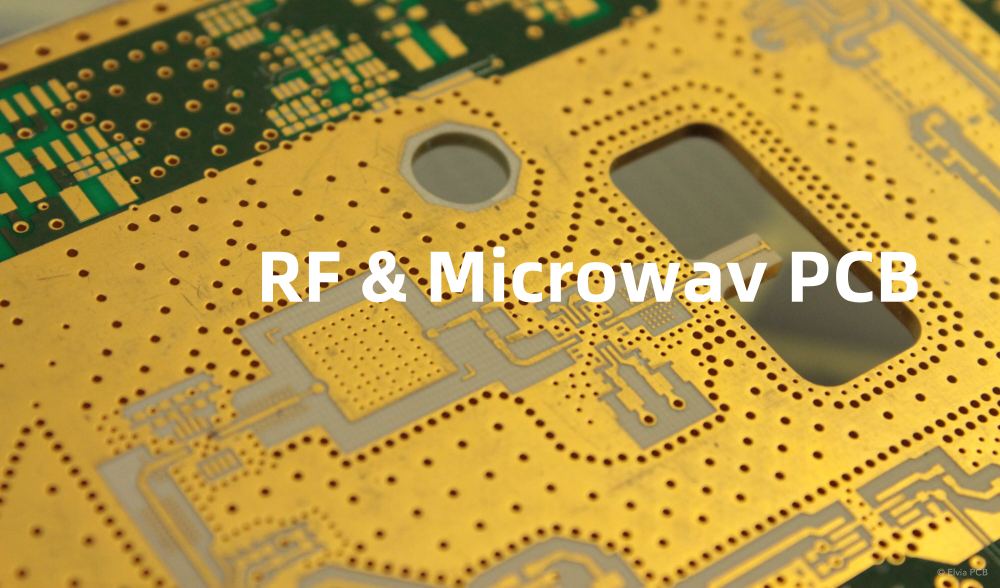
Printed Circuit Board (PCB) design is the process of creating the layout and interconnections for electronic components on a non-conductive substrate. PCBs are essential in modern electronics, providing a compact and efficient way to connect components. Designing PCBs involves several key considerations, such as component placement, routing, signal integrity, and manufacturability.
Types of PCBs
There are three main types of PCBs based on the number of layers:
- Single-layer PCBs
- Double-layer PCBs
- Multi-layer PCBs
| PCB Type | Layers | Complexity | Cost |
|---|---|---|---|
| Single-layer | 1 | Low | Low |
| Double-layer | 2 | Medium | Medium |
| Multi-layer | 3+ | High | High |
Multi-layer PCBs offer several advantages over single and double-layer PCBs, such as:
- Increased component density
- Improved signal integrity
- Better electromagnetic compatibility (EMC)
- Enhanced thermal management
Altium Designer for PCB Design
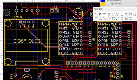
Altium Designer is a popular PCB design software that offers a comprehensive set of tools for schematic capture, PCB layout, and manufacturing preparation. It supports multi-layer PCB design and provides features like 3D visualization, design rule checking (DRC), and automatic routing.
Setting Up a Multi-layer PCB Project in Altium
To create a multi-layer PCB project in Altium Designer:
- Open Altium Designer and create a new project.
- Define the number of layers and their stack-up in the Layer Stack Manager.
- Set up design rules, such as Track width, clearance, and via sizes.
- Import or create the schematic and link it to the PCB layout.
- Place components and route the connections according to the design rules.
Ground Planes and Ground Free Areas
Ground planes are conductive layers in a PCB that provide a low-impedance return path for signals and help reduce electromagnetic interference (EMI). In multi-layer PCBs, one or more layers are often dedicated to ground planes.
However, there are situations where a ground free area (GFA) is required. A GFA is a region on the PCB where the ground plane is removed to avoid unwanted coupling between signals or to accommodate special components like antennas or high-voltage circuits.
Creating Ground Free Areas in Altium
To create a ground free area in Altium Designer:
- Select the layer on which you want to create the GFA.
- Use the polygon tool to draw the outline of the GFA.
- Set the polygon properties to “No Net” and assign a unique name to the polygon.
- Repeat the process for other layers if necessary.
| Layer | Polygon Name | Net |
|---|---|---|
| Top Layer | GFA_Top | No Net |
| Bottom Layer | GFA_Bottom | No Net |
Considerations for Ground Free Areas
When designing ground free areas, keep the following points in mind:
- Minimize the size of the GFA to avoid compromising the overall ground plane.
- Ensure adequate clearance between the GFA and surrounding components or traces.
- Consider the impact of the GFA on signal integrity and EMI.
- Verify the manufacturability of the design with the fabrication house.

Signal Integrity in Multi-layer PCBs
Signal integrity is a critical aspect of PCB design, especially in high-speed and high-frequency applications. Poor signal integrity can lead to issues like crosstalk, reflections, and EMI.
Factors Affecting Signal Integrity
Several factors can impact signal integrity in multi-layer PCBs:
- Trace geometry (width, thickness, and spacing)
- Dielectric material properties
- Via placement and design
- Termination and matching
- Power distribution network (PDN) design
Techniques for Improving Signal Integrity
To enhance signal integrity in multi-layer PCBs, consider the following techniques:
- Impedance control: Match the characteristic impedance of traces to the source and load impedances.
- Length matching: Ensure that traces carrying related signals have equal lengths to minimize skew.
- Differential pairs: Use differential signaling for high-speed interfaces to reduce EMI and improve noise immunity.
- Via optimization: Minimize the number of vias and optimize their placement to reduce discontinuities.
- Decoupling capacitors: Place decoupling capacitors close to ICs to suppress high-frequency noise.
Thermal Management in Multi-layer PCBs
Thermal management is another important consideration in multi-layer PCB design. As component density increases, heat generation becomes a significant concern. Proper thermal management helps ensure reliable operation and prevents premature component failure.
Thermal Vias and Copper Pours
Thermal vias and copper pours are two common techniques for improving heat dissipation in multi-layer PCBs:
- Thermal vias: These are vias placed beneath or around heat-generating components to transfer heat to other layers or the opposite side of the PCB.
- Copper pours: Large areas of copper are added to the PCB to spread heat more evenly and increase the overall thermal mass.
| Technique | Purpose | Placement |
|---|---|---|
| Thermal Vias | Transfer heat between layers | Beneath or around heat-generating components |
| Copper Pours | Spread heat evenly | Near heat-generating components or on dedicated layers |
Thermal Simulation and Analysis
Thermal simulation and analysis tools in Altium Designer help predict the temperature distribution and identify potential hot spots in the PCB. These tools allow designers to optimize the layout and cooling solutions before finalizing the design.
manufacturing Considerations for Multi-layer PCBs
Designing multi-layer PCBs for manufacturability is crucial to ensure a smooth transition from design to production. Collaborating with the fabrication house early in the design process can help avoid potential issues and delays.
Design for Manufacturing (DFM) Guidelines
Some essential DFM guidelines for multi-layer PCBs include:
- Adhering to the fabricator’s minimum feature sizes (trace width, spacing, and via diameter)
- Avoiding acute angles and maintaining consistent trace width
- Providing sufficient clearance around holes and vias
- Specifying the correct solder mask and silkscreen requirements
- Including fiducial markers and tooling holes for automated assembly
Panelization and Testing
Panelization is the process of arranging multiple PCBs on a single panel for fabrication. It helps optimize material usage and reduces manufacturing costs. When panelizing multi-layer PCBs, consider the following:
- Use mouse bites or V-grooves for easy separation of individual boards
- Provide adequate spacing between boards to avoid damage during depaneling
- Include test coupons or sacrificial areas for quality control purposes
Frequently Asked Questions (FAQ)
1. What is the minimum number of layers required for a multi-layer PCB?
A multi-layer PCB has three or more layers, with the most common configurations being 4, 6, 8, and 10 layers.
2. How does the number of layers affect the cost of a multi-layer PCB?
As the number of layers increases, the cost of the PCB also increases due to the additional materials, processing steps, and complexity involved in fabrication.
3. When should I consider using a ground free area in my PCB design?
Ground free areas are typically used when there is a need to isolate sensitive circuits, accommodate special components like antennas, or prevent unwanted coupling between signals.
4. What are some common signal integrity issues in multi-layer PCBs?
Common signal integrity issues in multi-layer PCBs include crosstalk, reflections, ground bounce, and electromagnetic interference (EMI).
5. How can I ensure my multi-layer PCB design is manufacturable?
To ensure manufacturability, follow the fabricator’s design for manufacturing (DFM) guidelines, communicate early with the fabrication house, and consider panelization and testing requirements.
Conclusion
Designing multi-layer PCBs and incorporating ground free areas using Altium Designer requires careful consideration of various factors, such as signal integrity, thermal management, and manufacturability. By understanding the principles of multi-layer PCB design, utilizing Altium Designer’s features, and collaborating with fabrication houses, designers can create reliable and high-performance electronic products.

No responses yet