Introduction to PTH PCB Technology
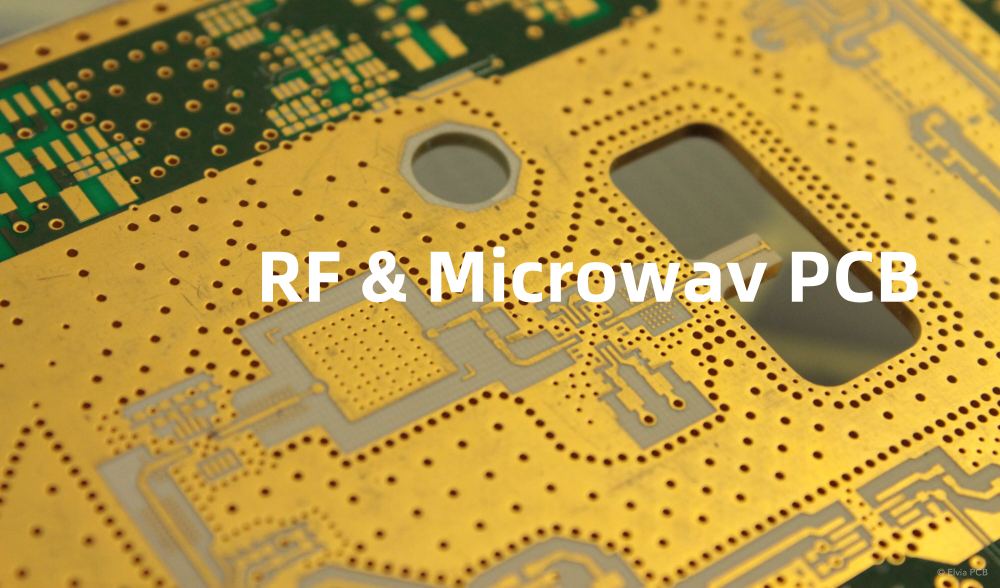
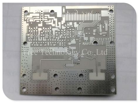
Plated through hole (PTH) is a crucial technology in the fabrication of printed circuit boards (PCBs). PTH PCBs have been widely used in the electronics industry for decades, providing reliable electrical connections between layers of a PCB. This technology involves drilling holes through the PCB substrate and plating them with a conductive material, typically copper, to create electrical connections between the layers.
The Importance of PTH in PCB Design
PTH technology plays a vital role in PCB design and manufacturing for several reasons:
-
Electrical Connectivity: PTH provides a reliable method for connecting different layers of a PCB, allowing signals and power to be routed efficiently.
-
Mechanical Strength: The plated holes offer mechanical support to the components mounted on the PCB, ensuring a stable and robust assembly.
-
Component Compatibility: Many electronic components, such as through-hole resistors, capacitors, and connectors, require PTH for proper mounting and electrical connection.
The PTH PCB Manufacturing Process
The manufacturing process for PTH PCBs involves several key steps:
1. Drilling
The first step in creating PTH PCBs is drilling holes through the substrate material. The holes are drilled using high-speed, computer-controlled drill machines, ensuring precise location and size.
2. Deburring and Cleaning
After drilling, the holes are deburred to remove any rough edges or debris. The PCB is then cleaned to remove any contaminants that may affect the plating process.
3. Electroless Copper Deposition
An electroless copper deposition process is used to create a thin, uniform layer of copper on the walls of the drilled holes and the surface of the PCB. This layer acts as a conductive base for the subsequent electroplating process.
4. Electroplating
The PCB is then placed in an electroplating bath, where a thicker layer of copper is deposited onto the electroless copper layer. This step ensures a reliable electrical connection and increases the mechanical strength of the plated holes.
5. Etching and Resist Stripping
After electroplating, the excess copper on the surface of the PCB is etched away, leaving only the desired copper traces and plated holes. The photoresist used to define the traces is then stripped away.
6. Solder Mask Application
A solder mask is applied to the surface of the PCB to protect the copper traces from oxidation and prevent solder bridges during the assembly process. The solder mask also provides electrical insulation between adjacent traces.
7. Surface Finish Application
A surface finish, such as HASL (Hot Air Solder Leveling), ENIG (Electroless Nickel Immersion Gold), or OSP (Organic Solderability Preservative), is applied to the exposed copper areas to protect them from oxidation and enhance solderability.
Advantages of PTH PCBs
PTH PCBs offer several advantages over other PCB technologies:
-
Reliability: PTH provides a robust and reliable electrical connection between layers, ensuring the proper functioning of the electronic device.
-
Mechanical Strength: The plated holes offer excellent mechanical support for components, making PTH PCBs suitable for applications that require high durability.
-
Versatility: PTH technology is compatible with a wide range of electronic components, making it a versatile choice for various applications.
-
Cost-effectiveness: For low-to-medium volume production, PTH PCBs can be a cost-effective solution compared to other technologies, such as surface mount technology (SMT).

Limitations of PTH PCBs
Despite their advantages, PTH PCBs also have some limitations:
-
Size Constraints: PTH components are generally larger than their surface mount counterparts, which can limit the miniaturization of electronic devices.
-
Higher Drilling Costs: The drilling process for PTH PCBs can be more time-consuming and expensive compared to other technologies, especially for high-density designs.
-
Limited High-Frequency Performance: PTH technology may not be suitable for high-frequency applications due to the inherent capacitance and inductance of the plated holes.
Applications of PTH PCBs
PTH PCBs are used in a wide range of applications, including:
-
Consumer Electronics: PTH PCBs are commonly used in consumer electronic devices, such as televisions, home appliances, and audio equipment.
-
Industrial Electronics: PTH technology is employed in industrial control systems, power supplies, and motor drives.
-
Automotive Electronics: PTH PCBs are used in various automotive electronic systems, such as engine control units, infotainment systems, and sensors.
-
Medical Devices: PTH PCBs are found in medical devices, including patient monitors, diagnostic equipment, and therapy devices.
Challenges and Future Trends
As the electronics industry continues to evolve, PCB manufacturers face several challenges and emerging trends:
-
Miniaturization: The demand for smaller, more compact electronic devices is driving the need for advanced PCB technologies that can accommodate higher component densities.
-
High-Frequency Applications: With the increasing use of high-frequency communication systems, such as 5G networks, PCB manufacturers must develop solutions that can handle higher frequencies and minimize signal integrity issues.
-
Environmental Concerns: The electronics industry is facing growing pressure to reduce its environmental impact. PCB manufacturers are exploring eco-friendly materials and processes to minimize waste and hazardous substances.
-
Intelligent Manufacturing: The adoption of Industry 4.0 technologies, such as the Internet of Things (IoT), artificial intelligence (AI), and machine learning (ML), is transforming PCB manufacturing processes, enabling greater automation, optimization, and quality control.
FAQ
1. What is the difference between PTH and SMT PCBs?
PTH (plated through hole) PCBs have components with leads that are inserted into drilled holes and soldered in place, while SMT (surface mount technology) PCBs have components that are soldered directly onto the surface of the board.
2. Can PTH and SMT components be used together on the same PCB?
Yes, PTH and SMT components can be combined on a single PCB, creating a hybrid design. This approach allows designers to leverage the advantages of both technologies while accommodating specific component requirements.
3. What is the minimum hole size for PTH PCBs?
The minimum hole size for PTH PCBs depends on various factors, such as the PCB Thickness, aspect ratio, and the capabilities of the PCB manufacturer. Typically, the minimum hole size ranges from 0.2mm to 0.3mm in diameter.
4. How does the PTH process affect the electrical properties of a PCB?
The PTH process can introduce additional capacitance and inductance to the PCB due to the presence of plated holes. These factors can impact the signal integrity and high-frequency performance of the PCB. Designers must consider these effects and employ appropriate design techniques to mitigate their impact.
5. Are there any specific design guidelines for PTH PCBs?
Yes, there are several design guidelines for PTH PCBs, including:
- Ensuring proper hole size and spacing to accommodate component leads
- Maintaining appropriate copper ring size around the holes for reliable soldering
- Considering the aspect ratio of the holes to ensure proper plating
- Following the manufacturer’s guidelines for minimum trace width and spacing
By adhering to these guidelines, designers can ensure the manufacturability and reliability of their PTH PCB designs.
Conclusion
Plated through hole (PTH) technology remains a crucial aspect of PCB Fabrication, offering reliable electrical connections, mechanical strength, and compatibility with a wide range of electronic components. Despite the challenges posed by miniaturization and high-frequency applications, PTH PCBs continue to be a preferred choice for many industries due to their cost-effectiveness and versatility.
As the electronics industry evolves, PCB manufacturers must adapt to new technologies and trends while addressing environmental concerns and embracing intelligent manufacturing processes. By understanding the advantages, limitations, and applications of PTH PCBs, designers and engineers can make informed decisions when selecting the most appropriate PCB technology for their projects.
| Characteristic | PTH PCBs | SMT PCBs |
|---|---|---|
| Component Mounting | Through holes | Surface mount |
| Hole Drilling | Required | Not required |
| Component Size | Larger | Smaller |
| Component Density | Lower | Higher |
| Manufacturing Cost | Higher for low-volume | Lower for high-volume |
| Suitability for High-Frequency | Limited | Better |
| Mechanical Strength | Higher | Lower |
| Rework and Repair | Easier | More challenging |
In summary, PTH PCB technology continues to play a vital role in the electronics industry, offering reliable and cost-effective solutions for a wide range of applications. As designers and manufacturers navigate the challenges and opportunities presented by emerging trends and technologies, a deep understanding of PTH PCBs remains essential for creating robust and efficient electronic devices.

No responses yet