Introduction to SMT Stencils and Laser-SMT-Stencils
Surface Mount Technology (SMT) has revolutionized the Electronics Manufacturing industry by enabling the production of smaller, faster, and more efficient electronic devices. One of the key components in the SMT Assembly process is the stencil, which is used to apply solder paste onto the printed circuit board (PCB) before placing the components. In this article, we will explore the world of SMT stencils, with a particular focus on laser-cut stencils, also known as Laser-SMT-Stencils.
What is an SMT Stencil?
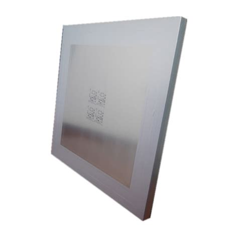
An SMT stencil is a thin sheet of metal, typically stainless steel, with precisely cut openings that correspond to the pads on a PCB. The stencil is placed over the PCB, and solder paste is applied using a squeegee or automated printer. The solder paste is forced through the openings in the stencil, depositing a precise amount of paste onto each pad. This process ensures that the correct amount of solder is applied to each component, which is crucial for achieving a reliable and high-quality solder joint.
Types of SMT Stencils
There are several types of SMT stencils available, each with its own advantages and disadvantages. The most common types include:
- Laser-cut stencils: These stencils are created using a high-precision laser cutting process, resulting in clean, sharp edges and tight tolerances. Laser-cut stencils are ideal for fine-pitch components and high-density PCB Layouts.
- Chemical-etched stencils: Chemical etching involves using a photoresist and chemical etchant to create the openings in the stencil. This process is less precise than laser cutting but is more cost-effective for larger openings and lower-density PCB layouts.
- Electroformed stencils: Electroforming is a process that uses electroplating to create a metal stencil with highly precise openings. This method is often used for ultra-fine pitch applications and can achieve even tighter tolerances than laser-cut stencils.
Advantages of Laser-SMT-Stencils
Laser-SMT-Stencils offer several key advantages over other types of SMT stencils:
High Precision and Accuracy
Laser cutting technology allows for extremely precise and accurate stencil openings, with tolerances as tight as ±0.0005 inches (±12.7 microns). This level of precision is essential for achieving reliable solder joints on fine-pitch components and high-density PCB layouts. Laser-cut stencils also have clean, sharp edges, which help to ensure a consistent solder paste deposit and minimize bridging between pads.
Durability and Long Service Life
Laser-SMT-Stencils are typically made from high-quality stainless steel, which is resistant to wear and tear, as well as corrosion from the solder paste. The laser cutting process also results in a smooth surface finish, which helps to prevent solder paste from sticking to the stencil and reduces the need for frequent cleaning. These factors contribute to a longer service life for laser-cut stencils compared to other types of stencils.
Rapid Prototyping and Quick Turnaround
The laser cutting process is highly automated and efficient, allowing for rapid prototyping and quick turnaround times. This is particularly beneficial for product development and low-volume production runs, where design changes may be frequent, and fast iteration is essential. Laser-SMT-Stencils can often be produced in a matter of days, compared to the weeks or even months required for other stencil manufacturing methods.
Versatility and Customization
Laser cutting technology is highly versatile and can accommodate a wide range of stencil thicknesses, aperture sizes, and shapes. This flexibility allows for the creation of custom stencil designs tailored to specific PCB layouts and component requirements. Laser-SMT-Stencils can also incorporate unique features, such as stepped apertures for different solder paste deposit heights, or relief cuts for improved paste release.

Stencil Design Considerations
To ensure optimal performance and reliability, several key factors must be considered when designing an SMT stencil, particularly for Laser-SMT-Stencils:
Stencil Thickness
The thickness of the stencil plays a crucial role in determining the amount of solder paste deposited on each pad. Thicker stencils will deposit more paste, while thinner stencils will deposit less. The optimal stencil thickness depends on several factors, including the size and pitch of the components, the PCB pad geometry, and the solder paste properties. As a general rule, stencil thickness should be between 60% and 90% of the minimum pad width.
| Component Pitch | Recommended Stencil Thickness |
|---|---|
| > 0.65 mm | 0.15 mm (6 mil) |
| 0.5 mm – 0.65 mm | 0.125 mm (5 mil) |
| 0.4 mm – 0.5 mm | 0.1 mm (4 mil) |
| < 0.4 mm | 0.08 mm (3 mil) |
Aperture Design
The size and shape of the stencil apertures directly influence the solder paste deposit. Apertures should be designed to match the size and shape of the PCB pads, with some additional considerations:
- Aperture size: For most applications, the aperture size should be slightly larger than the PCB pad to allow for proper paste release. A common rule of thumb is to add 10% to 20% to the pad dimensions.
- Aperture shape: Rectangular apertures are the most common, but other shapes, such as circles or ovals, may be used for specific components or to improve paste release.
- Aperture wall angle: The walls of the aperture should have a slight taper, typically 5° to 7°, to facilitate paste release and prevent clogging.
Area Ratio
Area ratio is a critical factor in determining the success of solder paste transfer through the stencil apertures. It is defined as the ratio of the aperture opening area to the aperture wall area. A higher area ratio indicates better paste release and less likelihood of clogging. As a general guideline, the area ratio should be at least 0.66 for reliable paste transfer.
Area Ratio = Aperture Opening Area / Aperture Wall Area
For example, consider a rectangular aperture with dimensions of 0.5 mm x 0.25 mm and a stencil thickness of 0.1 mm:
Aperture Opening Area = 0.5 mm × 0.25 mm = 0.125 mm²
Aperture Wall Area = 2 × (0.5 mm + 0.25 mm) × 0.1 mm = 0.15 mm²
Area Ratio = 0.125 mm² / 0.15 mm² = 0.83
In this case, the area ratio of 0.83 is sufficient for reliable solder paste transfer.

Stencil Manufacturing Process
The manufacturing process for Laser-SMT-Stencils involves several key steps:
- Material selection: High-quality stainless steel, typically grade 304 or 316, is used for its durability, corrosion resistance, and laser cutting performance.
- Cleaning and preparation: The stainless steel sheet is cleaned and inspected for any defects or irregularities that could affect the final stencil quality.
- Laser cutting: The stencil design is loaded into the laser cutting machine, which uses a high-power laser to precisely cut the apertures and features into the stainless steel sheet. The laser cutting process is computer-controlled, ensuring high accuracy and repeatability.
- Post-processing: After laser cutting, the stencil undergoes various post-processing steps, such as deburring, cleaning, and inspection. Any remaining burrs or rough edges are removed to ensure smooth aperture walls and optimal paste release.
- Quality control: The finished stencil is subjected to rigorous quality control measures, including dimensional verification, visual inspection, and paste transfer tests, to ensure that it meets the required specifications and performance criteria.

Stencil Maintenance and Handling
Proper maintenance and handling of Laser-SMT-Stencils are essential for ensuring consistent performance and long service life:
Cleaning
Regular cleaning of the stencil is necessary to remove solder paste residue and prevent clogging of the apertures. Several cleaning methods can be employed, depending on the severity of the contamination and the available resources:
- Manual cleaning: For light contamination, manual cleaning with isopropyl alcohol (IPA) and a lint-free wipe can be effective. The stencil should be wiped in a single direction to avoid pushing residue back into the apertures.
- Ultrasonic cleaning: For more stubborn residue, ultrasonic cleaning in a bath of IPA or a specialized stencil cleaning solution can be used. The stencil is immersed in the cleaning solution and subjected to high-frequency vibrations, which help to dislodge the residue.
- Automated cleaning: For high-volume production, automated stencil cleaning systems can be employed. These systems typically use a combination of spray washing, brushing, and drying to clean the stencil quickly and efficiently.
Storage and Handling
Proper storage and handling of Laser-SMT-Stencils can help to prevent damage and extend their service life:
- Storage: Stencils should be stored in a clean, dry environment, away from direct sunlight and sources of heat or humidity. They should be kept in protective packaging or containers to prevent scratches, dents, or other physical damage.
- Handling: When handling stencils, care should be taken to avoid bending, twisting, or subjecting them to excessive force. Gloves should be worn to prevent contamination from skin oils and debris.
- Inspection: Regular inspection of the stencil for signs of wear, damage, or contamination can help to identify potential issues before they lead to defects in the solder paste printing process.
Troubleshooting Common Stencil Issues
Despite proper design, manufacturing, and maintenance, issues can still arise with Laser-SMT-Stencils. Some common problems and their potential solutions include:
Insufficient Solder Paste Deposit
If the solder paste deposit is too small or inconsistent, it may be due to:
- Clogged apertures: Clean the stencil thoroughly, using the appropriate cleaning method for the level of contamination.
- Low area ratio: Redesign the apertures to increase the area ratio, or consider using a thinner stencil.
- Worn or damaged squeegee: Replace the squeegee with a new one, ensuring that it is the correct size, material, and durometer for the application.
Excessive Solder Paste Deposit
If the solder paste deposit is too large or inconsistent, it may be due to:
- Overprinting: Adjust the printer settings, such as squeegee pressure, speed, and separation distance, to reduce the amount of paste deposited.
- Stencil warpage: Inspect the stencil for warpage and replace it if necessary. Ensure that the stencil is properly mounted and tensioned in the printer.
- Excessive stencil thickness: Consider using a thinner stencil, or redesign the apertures to compensate for the increased paste volume.
Solder Paste Bridging
If solder paste is bridging between pads, it may be due to:
- Insufficient aperture spacing: Increase the spacing between apertures, or consider using a stepped stencil to reduce the paste volume on adjacent pads.
- Poor paste release: Ensure that the aperture walls are smooth and tapered, and that the area ratio is sufficient for reliable paste release. Clean the stencil thoroughly to remove any residue that may be impeding paste release.
- Incorrect squeegee parameters: Adjust the squeegee pressure, speed, and angle to improve paste release and minimize bridging.
Frequently Asked Questions (FAQ)
-
Q: What is the difference between a laser-cut stencil and a chemical-etched stencil?
A: Laser-cut stencils are created using a high-precision laser cutting process, resulting in clean, sharp edges and tight tolerances. Chemical-etched stencils are made by using a photoresist and chemical etchant to create the apertures, which is less precise but more cost-effective for larger openings and lower-density PCB layouts. -
Q: How long does a Laser-SMT-Stencil typically last?
A: The lifespan of a Laser-SMT-Stencil depends on various factors, such as the stencil material, thickness, aperture design, and maintenance practices. With proper care and handling, a laser-cut stencil can typically last for several thousand prints or more. -
Q: Can Laser-SMT-Stencils be used for multiple PCB designs?
A: While it is possible to use a single stencil for multiple PCB designs, it is generally recommended to use a dedicated stencil for each design to ensure optimal performance and paste deposit accuracy. Using a stencil designed specifically for a given PCB layout will provide the best results. -
Q: How often should a Laser-SMT-Stencil be cleaned?
A: The frequency of cleaning depends on the production volume, solder paste type, and environmental conditions. As a general guideline, stencils should be cleaned every 4-8 hours of continuous use, or whenever a visible buildup of solder paste residue is observed. More frequent cleaning may be necessary for high-volume production or when using no-clean solder pastes. -
Q: Can Laser-SMT-Stencils be repaired if damaged?
A: In most cases, damaged Laser-SMT-Stencils cannot be effectively repaired and must be replaced. Minor damage, such as small dents or scratches, may not significantly impact performance, but more severe damage, such as large creases or warpage, will likely require stencil replacement to maintain print quality and consistency.
Conclusion
Laser-SMT-Stencils are a critical component in the SMT assembly process, enabling the precise and consistent application of solder paste to PCB pads. By understanding the advantages, design considerations, manufacturing process, and maintenance requirements of laser-cut stencils, engineers and manufacturers can optimize their SMT production and achieve high-quality, reliable solder joints.
As the electronics industry continues to push the boundaries of miniaturization and performance, the demand for high-precision Laser-SMT-Stencils will only continue to grow. By staying up-to-date with the latest developments in stencil technology and best practices, manufacturers can ensure that they are well-positioned to meet the challenges of the evolving SMT landscape.
No responses yet