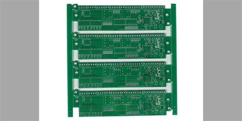
What is PCB Silkscreen Printing?
PCB silkscreen printing is a method used to apply text, logos, and other markings onto printed circuit boards. It involves using a fine mesh screen and a squeegee to transfer ink onto specific areas of the PCB surface. The screen acts as a stencil, allowing ink to pass through the open areas while blocking it in the solid regions.
The silkscreen printing process offers several advantages for PCB marking:
- Durability: Silkscreen ink is resistant to abrasion, chemicals, and high temperatures, ensuring the markings remain legible throughout the PCB’s lifespan.
- Precision: The fine mesh screen allows for high-resolution printing, enabling the application of detailed text and graphics.
- Versatility: Silkscreen printing can be used on various PCB materials, including FR-4, aluminum, and flexible substrates.
- Cost-effectiveness: Compared to other marking methods, silkscreen printing is relatively inexpensive, especially for large production runs.
Applications of PCB Silkscreen Printing
PCB silkscreen printing is used for several purposes:
Component Identification
One of the primary applications of silkscreen printing is to label components on the PCB. This includes:
- Reference designators (e.g., R1, C2, U3) to identify individual components
- Polarity markings (e.g., + and -) for capacitors and diodes
- Pin numbers for integrated circuits and connectors
Having clear component labels helps during PCB Assembly, testing, and repair.
Orientation and Assembly Instructions
Silkscreen markings can provide visual cues for proper PCB orientation and assembly:
- Board outline and mounting hole locations
- Connector and switch positions
- Recommended component placement directions
- Warning labels (e.g., “High Voltage” or “ESD Sensitive”)
These markings ensure the correct assembly of the PCB and prevent potential damage during handling.
Branding and Aesthetics
Silkscreen printing allows for the application of company logos, product names, and other branding elements on the PCB. This helps in product identification and enhances the overall aesthetics of the board.
Regulatory Compliance
Certain industries, such as medical and aerospace, require Specific markings on PCBs for traceability and compliance purposes. Silkscreen printing can be used to apply:
- Serial numbers and batch codes
- Certification marks (e.g., UL, CE, RoHS)
- Country of origin
- Date of manufacture
Having these markings ensures the PCB meets the necessary regulatory requirements.

The PCB Silkscreen Printing Process
The silkscreen printing process involves several steps:
-
Artwork Preparation: The desired markings are designed using CAD software, and the artwork is created in a format suitable for screen printing (e.g., vector or high-resolution raster images).
-
Screen Preparation: A fine mesh screen, typically made of polyester or stainless steel, is coated with a light-sensitive emulsion. The artwork is then exposed onto the screen, hardening the emulsion in the non-image areas. The unexposed emulsion is washed away, leaving open areas for the ink to pass through.
-
Ink Selection: The type of ink used depends on the PCB material, the desired color, and the required durability. Common ink types include epoxy, UV-curable, and solvent-based inks.
-
Printing: The prepared screen is placed over the PCB, and ink is applied to one end of the screen. A squeegee is then used to push the ink through the open areas of the screen and onto the PCB surface. The screen is lifted, leaving the ink on the board.
-
Curing: The printed ink is cured to ensure proper adhesion and durability. Curing methods vary depending on the ink type and can include air drying, oven baking, or UV exposure.
-
Inspection: The printed PCBs are inspected for defects, such as incomplete or smudged markings. Automated optical inspection (AOI) systems can be used for high-volume production.

Factors Affecting PCB Silkscreen Print Quality
Several factors can influence the quality of silkscreen printing on PCBs:
Screen Mesh Count
The mesh count of the screen determines the resolution and ink deposit thickness of the print. Higher mesh counts (e.g., 200-400 threads per inch) allow for finer details but may require thinner inks. Lower mesh counts (e.g., 80-160 threads per inch) are suitable for larger, bolder markings.
Ink Properties
The ink’s viscosity, surface tension, and drying time can affect print quality. Inks with high viscosity or surface tension may not flow easily through the screen, resulting in incomplete or uneven prints. Fast-drying inks can clog the screen, while slow-drying inks may smudge or blur.
PCB Surface Finish
The surface finish of the PCB can impact ink adhesion and print quality. Smooth, non-porous finishes like HASL (Hot Air Solder Leveling) and ENIG (Electroless Nickel Immersion Gold) are generally easier to print on compared to rough or porous finishes like OSP (Organic Solderability Preservative).
Squeegee Pressure and Angle
The pressure and angle of the squeegee during printing can affect ink deposit thickness and consistency. Too much pressure can cause ink to bleed or smudge, while insufficient pressure may result in incomplete prints. The optimal squeegee angle is typically between 45-60 degrees.
Environmental Conditions
Temperature and humidity can influence ink drying time and print quality. High humidity can cause ink to dry slowly or blur, while low humidity may lead to premature screen drying and clogging. Maintaining a controlled environment with proper ventilation can help mitigate these issues.

Common PCB Silkscreen Printing Defects and Solutions
Despite careful process control, various defects can occur during silkscreen printing:
| Defect | Description | Possible Causes | Solutions |
|---|---|---|---|
| Incomplete or missing print | Parts of the markings are missing or not fully printed | – Clogged screen – Low ink viscosity – Insufficient squeegee pressure |
– Clean or replace the screen – Adjust ink viscosity – Increase squeegee pressure |
| Smudging or blurring | Markings have fuzzy edges or are smeared | – High ink viscosity – Slow ink drying – Excessive squeegee pressure |
– Reduce ink viscosity – Use faster-drying ink or adjust curing conditions – Decrease squeegee pressure |
| Misalignment | Markings are not in the correct position relative to the PCB features | – Improper screen alignment – PCB misregistration – Artwork error |
– Verify screen alignment – Check PCB positioning and fixturing – Review and correct artwork |
| Inconsistent ink thickness | Markings have uneven or varying ink deposit | – Worn or damaged squeegee – Inconsistent squeegee pressure – Uneven PCB surface |
– Replace the squeegee – Maintain consistent pressure during printing – Ensure PCB surface is clean and level |
By identifying the root causes of these defects and implementing appropriate solutions, PCB manufacturers can improve the quality and consistency of their silkscreen printing process.
Frequently Asked Questions (FAQ)
1. What is the minimum font size for PCB silkscreen printing?
The minimum font size for silkscreen printing depends on the screen mesh count and ink properties. Generally, a font size of 0.8mm (0.032 inches) or larger is recommended for legibility. Smaller font sizes may be possible with high mesh count screens and fine-detail inks, but they may be more challenging to print consistently.
2. Can silkscreen printing be used on both sides of the PCB?
Yes, silkscreen printing can be applied to both the top and bottom sides of the PCB. However, it is essential to ensure proper alignment and registration between the two sides to avoid any discrepancies in the markings.
3. How durable are silkscreen markings on PCBs?
Silkscreen markings are highly durable and can withstand exposure to solvents, abrasion, and high temperatures. The durability of the markings depends on the type of ink used and the curing process. Epoxy and UV-curable inks are known for their excellent adhesion and resistance properties.
4. Can silkscreen printing be used for solder mask application?
No, silkscreen printing is not suitable for solder mask application. Solder masks are typically applied using screen printing or photoimaging processes, which involve different materials and curing methods compared to silkscreen inks.
5. Are there any alternatives to silkscreen printing for PCB marking?
Yes, there are several alternatives to silkscreen printing for PCB marking, including:
- Laser marking: Uses a laser to etch or discolor the PCB surface
- Direct inkjet printing: Deposits ink directly onto the PCB using a high-resolution inkjet printer
- Label printing: Involves printing on a separate label and applying it to the PCB surface
Each method has its own advantages and limitations, and the choice depends on factors such as production volume, marking requirements, and cost considerations.
Conclusion
PCB silkscreen printing is a versatile and cost-effective method for applying text, logos, and other markings onto printed circuit boards. It plays a crucial role in component identification, assembly instructions, branding, and regulatory compliance.
By understanding the silkscreen printing process, factors affecting print quality, and common defects, PCB manufacturers can optimize their marking operations and ensure consistent, high-quality results. As PCB designs continue to evolve and become more complex, the importance of clear and durable silkscreen markings will only increase.
Investing in the right equipment, materials, and process control measures can help PCB manufacturers stay competitive and meet the ever-growing demands of the electronics industry.
No responses yet