What is Reflow Soldering?
Reflow soldering is a process used in the manufacturing of printed Circuit Boards (PCBs) to attach surface mount components to the board. It involves applying solder paste to the PCB, placing the components onto the paste, and then heating the entire assembly in a reflow oven to melt the solder and create a permanent connection between the components and the board.
Reflow soldering is widely used in the electronics industry because it allows for the efficient and precise placement of small components onto PCBs. It is particularly useful for high-volume production runs, as it can be automated and optimized for speed and accuracy.
Advantages of Reflow Soldering
- High-speed production: Reflow soldering allows for the rapid assembly of PCBs, making it ideal for high-volume manufacturing.
- Precision: The use of solder paste and automated component placement ensures precise and consistent connections between components and the PCB.
- Repeatability: Reflow soldering processes can be easily replicated, ensuring consistent quality across multiple production runs.
- Versatility: Reflow soldering can be used with a wide range of component sizes and types, making it suitable for a variety of PCB Designs.
The Reflow Soldering Process
The reflow soldering process consists of several key steps:
- Solder paste application
- Component placement
- Reflow oven heating
- Cooling and inspection
1. Solder Paste Application
Solder paste is a mixture of tiny solder particles suspended in a flux medium. It is applied to the PCB using a stencil or screen printing process. The stencil is a thin metal sheet with openings that correspond to the pads on the PCB where the components will be placed. The solder paste is forced through the openings onto the pads, creating a precise deposit of paste on each pad.
Solder Paste Composition
Solder paste typically consists of the following components:
- Solder alloy particles (usually tin, lead, and silver)
- Flux (to remove oxides and improve solder wetting)
- Solvents (to control viscosity and improve printability)
- Additives (to enhance performance and shelf life)
The composition of the solder paste can be adjusted to suit the specific requirements of the PCB design and the reflow soldering process.
2. Component Placement
Once the solder paste has been applied to the PCB, the surface mount components are placed onto the pads. This is usually done using an automated pick-and-place machine, which uses vacuum nozzles to pick up the components from tape reels or trays and place them onto the PCB with high precision.
The accuracy of component placement is critical to the success of the reflow soldering process. Misaligned or incorrectly placed components can lead to poor solder joints, short circuits, or other defects.
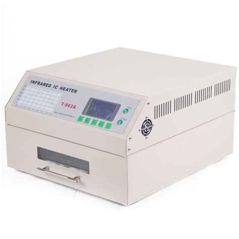
3. Reflow Oven Heating
After the components have been placed, the PCB Assembly is passed through a reflow oven. The oven heats the assembly in a controlled manner, following a specific temperature profile that is designed to melt the solder paste and form a strong bond between the components and the PCB.
Reflow Temperature Profile
The reflow temperature profile is a critical aspect of the reflow soldering process. It defines the temperature and duration of each stage of the heating process, ensuring that the solder melts and flows correctly without damaging the components or the PCB.
A typical reflow temperature profile consists of four stages:
- Preheat: The assembly is gradually heated to a temperature just below the melting point of the solder. This stage helps to evaporate solvents and activate the flux in the solder paste.
- Thermal soak: The assembly is held at a stable temperature to ensure that all components and the PCB reach a uniform temperature.
- Reflow: The temperature is rapidly increased above the melting point of the solder, causing the solder to melt and flow around the component leads and the PCB pads.
- Cooling: The assembly is cooled at a controlled rate to allow the solder to solidify and form a strong, reliable joint.
The specific temperatures and durations of each stage will depend on factors such as the type of solder paste being used, the size and thermal mass of the components, and the design of the PCB.
| Stage | Temperature Range (°C) | Duration (seconds) |
|---|---|---|
| Preheat | 150-180 | 60-120 |
| Thermal Soak | 180-200 | 60-120 |
| Reflow | 220-250 | 30-60 |
| Cooling | 250-room temperature | 60-120 |
Example of a typical reflow temperature profile
4. Cooling and Inspection
After the reflow process is complete, the PCB assembly is allowed to cool naturally or with the aid of forced air cooling. As the solder solidifies, it forms a strong mechanical and electrical connection between the components and the PCB.
Once cooled, the PCB assembly undergoes a visual inspection to check for any defects or issues with the solder joints. Common defects include:
- Bridging: Solder bridges form between adjacent pads or pins.
- Tombstoning: Components stand up on one end due to uneven heating or solder wetting.
- Insufficient solder: Solder joints are weak or incomplete due to insufficient solder paste.
- Solder balls: Small balls of solder form on the PCB surface or component leads.
If any defects are found, the PCB may need to be reworked or scrapped, depending on the severity of the issue.

Factors Affecting Reflow Soldering Quality
Several factors can impact the quality of the reflow soldering process and the resulting solder joints:
- Solder paste quality: The composition, viscosity, and particle size of the solder paste can affect its printability, wetting behavior, and melting characteristics.
- Stencil design: The openings in the stencil must be properly sized and positioned to ensure the correct amount of solder paste is deposited on each pad.
- Component placement accuracy: Misaligned or improperly seated components can lead to poor solder joints or other defects.
- Reflow temperature profile: The heating and cooling rates, as well as the peak temperature and duration, must be carefully controlled to ensure proper solder melting and flow without damaging the components or PCB.
- PCB design: The layout and spacing of components, as well as the size and shape of the pads, can affect the ease and reliability of the reflow soldering process.
By carefully controlling these factors and following best practices for reflow soldering, manufacturers can ensure high-quality, reliable PCB assemblies.

Best Practices for Reflow Soldering
To achieve the best results from the reflow soldering process, consider the following best practices:
- Use high-quality solder paste with the appropriate composition and particle size for your application.
- Design stencils with properly sized and positioned openings to ensure consistent solder paste deposition.
- Use automated pick-and-place machines to ensure precise and repeatable component placement.
- Develop and optimize your reflow temperature profile based on the specific requirements of your PCB design and components.
- Regularly maintain and calibrate your reflow oven to ensure consistent and accurate heating.
- Implement a robust inspection and quality control process to identify and address any defects or issues with the solder joints.

Troubleshooting Common Reflow Soldering Issues
Despite best efforts, issues can sometimes arise during the reflow soldering process. Here are some common problems and potential solutions:
| Issue | Possible Causes | Solutions |
|---|---|---|
| Solder bridging | – Excessive solder paste – Improperly sized stencil openings – Incorrect reflow temperature profile |
– Adjust solder paste volume – Modify stencil design – Optimize reflow temperature profile |
| Tombstoning | – Uneven heating of components – Improperly sized or shaped pads – Incorrect component placement |
– Adjust reflow temperature profile – Modify pad design – Improve component placement accuracy |
| Insufficient solder | – Insufficient solder paste – Improperly sized stencil openings – Incorrect reflow temperature profile |
– Increase solder paste volume – Modify stencil design – Optimize reflow temperature profile |
| Solder balls | – Contaminated or oxidized PCB or components – Excessive solder paste – Incorrect reflow temperature profile |
– Clean PCB and components – Adjust solder paste volume – Optimize reflow temperature profile |
By understanding the root causes of these issues and implementing appropriate solutions, manufacturers can minimize defects and improve the overall quality of their reflow soldered PCB assemblies.
Frequently Asked Questions (FAQ)
-
What is the difference between reflow soldering and Wave Soldering?
Reflow soldering is used for surface mount components and involves applying solder paste to the PCB, placing the components, and heating the assembly in a reflow oven. Wave soldering, on the other hand, is used for through-hole components and involves passing the PCB over a molten solder wave to create the solder joints. -
Can reflow soldering be used for through-hole components?
While reflow soldering is primarily used for surface mount components, it can be used for some through-hole components with appropriate adaptations. However, wave soldering is generally more suitable for through-hole components. -
What is the purpose of flux in solder paste?
Flux serves several purposes in solder paste: it removes oxides from the surfaces of the PCB and component leads, improves the wetting and flow of the molten solder, and helps to prevent re-oxidation during the soldering process. -
How do I select the right solder paste for my application?
When selecting a solder paste, consider factors such as the alloy composition (e.g., tin-lead or lead-free), particle size, flux type (e.g., rosin-based or no-clean), and viscosity. Consult with your solder paste supplier or manufacturer for guidance on selecting the most suitable product for your specific application. -
How often should I calibrate my reflow oven?
The frequency of reflow oven calibration depends on factors such as the usage intensity, environmental conditions, and manufacturer recommendations. As a general guideline, it is advisable to calibrate your reflow oven at least once every six months or whenever you notice inconsistencies in the soldering process or product quality.
Conclusion
Reflow soldering is a critical process in the manufacturing of high-quality, reliable PCB assemblies. By understanding the key steps involved, controlling the various factors that affect soldering quality, and following best practices, manufacturers can optimize their reflow soldering processes to achieve consistent and defect-free results.
Regular maintenance, calibration, and troubleshooting, along with a commitment to continuous improvement, will help to ensure the long-term success and efficiency of your reflow soldering operations.
No responses yet