Introduction to CAD2CAM4PCB
CAD2CAM4PCB is a comprehensive software solution for designing and manufacturing printed circuit boards (PCBs). It bridges the gap between computer-aided design (CAD) and computer-aided manufacturing (CAM) in the PCB industry. The software streamlines the PCB design and manufacturing process, enabling users to create high-quality PCB designs and generate the necessary files for manufacturing.
Key Features of CAD2CAM4PCB
-
Schematic Capture: CAD2CAM4PCB provides a user-friendly schematic capture tool that allows designers to create electronic schematics quickly and efficiently. It supports various schematic symbols, net labels, and hierarchical design capabilities.
-
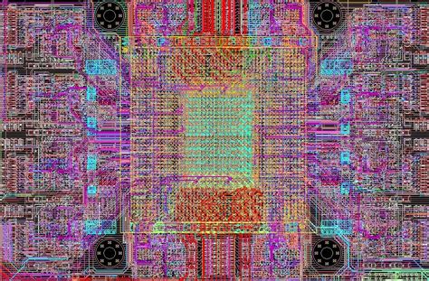
PCB Layout: The software offers a powerful PCB layout editor with advanced features such as auto-routing, design rule checking (DRC), and real-time 3D visualization. It supports multi-layer PCB designs and provides tools for placement, routing, and copper pour.
-
Library Management: CAD2CAM4PCB includes an extensive library of components, footprints, and symbols. Users can easily manage and customize their libraries, ensuring consistency and accuracy across their designs.
-
Design Rule Checking: The built-in DRC feature checks the PCB design against a set of predefined or user-defined rules to identify potential issues such as shorts, opens, and manufacturability problems. This helps ensure the integrity and reliability of the final PCB.
-
Manufacturing Output: CAD2CAM4PCB generates the necessary manufacturing files, including Gerber files, drill files, and assembly drawings. These files can be directly sent to PCB manufacturers for production.
Benefits of Using CAD2CAM4PCB
Increased Efficiency and Productivity
CAD2CAM4PCB significantly improves the efficiency and productivity of the PCB design process. Its intuitive interface and automated features, such as auto-routing and design rule checking, save time and reduce the manual effort required. Designers can focus on the creative aspects of PCB design while the software handles tedious tasks.
Enhanced Design Quality
The software’s comprehensive design rule checking capabilities help identify and resolve potential issues early in the design process. This leads to higher-quality PCB designs with fewer errors and improved manufacturability. CAD2CAM4PCB’s real-time 3D visualization feature allows designers to visually inspect their designs, ensuring proper component placement and clearance.
Seamless Integration with Manufacturing
CAD2CAM4PCB generates industry-standard manufacturing files, such as Gerber and drill files, that can be directly used by PCB manufacturers. This seamless integration eliminates the need for manual file conversion and reduces the risk of errors during the manufacturing process. The software ensures that the manufactured PCB accurately reflects the original design intent.
Cost Savings
By streamlining the PCB design and manufacturing process, CAD2CAM4PCB helps reduce overall costs. The software’s automation features minimize the time and resources required for design iterations and revisions. Its design rule checking capabilities catch potential issues early, avoiding costly manufacturing mistakes and rework.

CAD2CAM4PCB Seminar Overview
A recent seminar on CAD2CAM4PCB was held to introduce the software to PCB designers, engineers, and industry professionals. The seminar aimed to showcase the capabilities of CAD2CAM4PCB and provide hands-on experience to the attendees.
Seminar Agenda
The CAD2CAM4PCB seminar covered the following topics:
| Topic | Duration |
|---|---|
| Introduction to CAD2CAM4PCB | 30 min |
| Schematic Capture Demonstration | 45 min |
| PCB Layout Design Techniques | 60 min |
| Design Rule Checking and Optimization | 45 min |
| Generating Manufacturing Files | 30 min |
| Q&A Session | 30 min |
Attendee Feedback
The seminar received positive feedback from the attendees, who appreciated the comprehensive coverage of CAD2CAM4PCB’s features and the practical demonstrations. Many attendees expressed their interest in adopting the software in their own design workflows.
Here are some notable quotes from the attendees:
- “CAD2CAM4PCB seems to be a game-changer in PCB design. The automated features and intuitive interface can greatly enhance productivity.” – John Smith, Senior PCB Designer
- “The real-time 3D visualization is impressive. It helps in identifying potential issues and ensures a smooth transition to manufacturing.” – Emily Johnson, Hardware Engineer
- “The seamless integration with manufacturing is a significant advantage. It eliminates the hassle of file conversion and reduces the chances of errors.” – Michael Davis, Production Manager

Case Studies
Several companies have successfully implemented CAD2CAM4PCB in their PCB design and manufacturing processes. Here are two notable case studies:
Case Study 1: ABC Electronics
ABC Electronics, a leading manufacturer of consumer electronics, adopted CAD2CAM4PCB to streamline their PCB design process. By utilizing the software’s auto-routing and design rule checking features, they were able to reduce their design cycle time by 30%. The seamless integration with their manufacturing workflow resulted in a 20% reduction in production errors and rework.
Case Study 2: XYZ Robotics
XYZ Robotics, a startup specializing in robotic systems, used CAD2CAM4PCB to design complex PCBs for their products. The software’s extensive component library and real-time 3D visualization capabilities allowed their designers to create compact and high-performance PCBs. The generated manufacturing files were directly sent to their PCB fabrication partner, resulting in faster prototyping and shorter time-to-market.

Frequently Asked Questions (FAQ)
-
Is CAD2CAM4PCB suitable for beginners?
Yes, CAD2CAM4PCB has a user-friendly interface and provides tutorials and documentation to help beginners get started. The software’s intuitive tools and automated features make it accessible to users with varying levels of experience. -
Can CAD2CAM4PCB handle complex PCB designs?
Absolutely. CAD2CAM4PCB is designed to handle both simple and complex PCB designs. It supports multi-layer PCBs, high-density layouts, and advanced routing techniques. The software’s design rule checking capabilities ensure the manufacturability of even the most complex designs. -
Does CAD2CAM4PCB support custom component libraries?
Yes, CAD2CAM4PCB allows users to create and manage their own custom component libraries. Users can import existing libraries or create new components from scratch. The software provides a library management system to organize and share components across projects. -
Can CAD2CAM4PCB generate assembly drawings?
Yes, CAD2CAM4PCB can generate assembly drawings along with other manufacturing files. Assembly drawings provide clear instructions for component placement and orientation, aiding in the PCB Assembly process. -
Is there a free trial version of CAD2CAM4PCB available?
Yes, a free trial version of CAD2CAM4PCB is available for download from the official website. The trial version allows users to explore the software’s features and evaluate its suitability for their specific needs before making a purchase decision.
Conclusion
CAD2CAM4PCB is a powerful software solution that streamlines the PCB design and manufacturing process. Its comprehensive features, including schematic capture, PCB layout, design rule checking, and manufacturing file generation, make it an invaluable tool for PCB designers and engineers.
The recent CAD2CAM4PCB seminar highlighted the software’s capabilities and received positive feedback from attendees. Case studies demonstrate the tangible benefits of implementing CAD2CAM4PCB, such as reduced design cycle time, improved design quality, and seamless integration with manufacturing.
As the demand for efficient and reliable PCB design solutions continues to grow, CAD2CAM4PCB is well-positioned to meet the needs of the industry. Its user-friendly interface, automated features, and comprehensive functionality make it a top choice for companies looking to optimize their PCB design and manufacturing processes.
No responses yet