What is a PCB Visualizer?
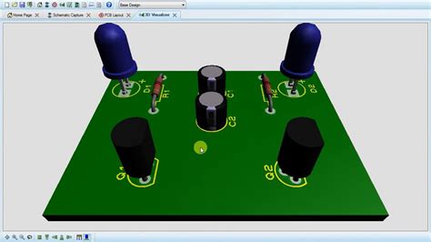
A PCB (printed circuit board) visualizer is a software tool that allows engineers and designers to view and analyze a PCB design in 3D. It provides a realistic representation of the PCB, including all components, copper traces, vias, and other features. The visualizer helps identify potential issues early in the design process, saving time and reducing the risk of costly mistakes.
Benefits of Using a PCB Visualizer
There are many benefits to using a PCB visualizer in the design process:
-
Improved Design Quality: By seeing the PCB in 3D, designers can identify and fix problems such as component collisions, insufficient clearances, and manufacturing constraints before sending the design to production. This results in higher quality boards that are less likely to have issues.
-
Faster Iteration: With a PCB visualizer, designers can quickly make changes to the layout and see the results in real-time. This allows for faster iteration and optimization of the design.
-
Better Communication: A 3D visualization of the PCB makes it easier to communicate the design intent to stakeholders, such as manufacturers, assemblers, and customers. It provides a clear and unambiguous representation of the board that everyone can understand.
-
Enhanced Collaboration: PCB visualizers often include collaboration features that allow multiple designers to work on the same project simultaneously. This can speed up the design process and ensure that everyone is working towards the same goal.
How Does a PCB Visualizer Work?
A PCB visualizer works by taking the design data from a PCB design tool, such as Altium Designer or KiCad, and rendering it in 3D. The visualizer uses the information in the design files, such as the component footprints, copper traces, and board stackup, to create an accurate representation of the PCB.
Importing Design Data
The first step in using a PCB visualizer is to import the design data from the PCB design tool. This is typically done using a common file format, such as ODB++, IPC-2581, or Gerber. The visualizer reads the design data and creates a 3D model of the PCB.
Navigating the 3D Model
Once the 3D model is created, designers can navigate around it using the visualizer’s controls. This typically includes the ability to rotate, zoom, and pan the view to see the board from different angles. Some visualizers also allow designers to slice through the board to see the internal layers and cross-sections.
Analyzing the Design
With the 3D model loaded, designers can use the visualizer’s analysis tools to check the design for potential issues. This may include:
- Checking for component collisions and insufficient clearances
- Verifying that the copper traces meet the design rules for width, spacing, and impedance
- Analyzing the board stackup to ensure proper layer alignment and thickness
- Checking for manufacturability issues, such as drill sizes and solder mask clearances
Making Changes
If issues are found during the analysis, designers can use the visualizer to make changes to the design. Some visualizers include built-in editing tools that allow designers to move components, resize pads, and adjust trace routing directly in the 3D view. Others integrate with the PCB design tool, allowing designers to make changes in the design tool and see the results in the visualizer.

Common Features of PCB Visualizers
While the specific features of PCB visualizers vary by product, there are some common capabilities that most tools offer:
3D Rendering
All PCB visualizers provide a 3D rendering of the PCB design. The quality and accuracy of the rendering varies by tool, but most offer a realistic representation of the board that includes components, copper traces, silk screen, and solder mask.
Real-Time Interaction
Many PCB visualizers allow designers to interact with the 3D model in real-time. This may include the ability to rotate, zoom, and pan the view, as well as select and highlight individual components and nets.
Analysis Tools
PCB visualizers typically include a range of analysis tools that help designers check the design for potential issues. These may include:
- Design rule checking (DRC) to verify that the design meets the specified constraints for trace width, spacing, and clearance
- Electrical rule checking (ERC) to analyze the schematic and ensure that the design is electrically correct
- Signal integrity analysis to simulate the behavior of high-speed signals and identify potential issues such as crosstalk and reflections
- Thermal analysis to predict the temperature distribution on the board and identify hot spots that may affect reliability
Collaboration Features
Some PCB visualizers include collaboration features that allow multiple designers to work on the same project simultaneously. This may include the ability to share the 3D model, make comments and annotations, and track changes made by each team member.
Integration with Other Tools
Many PCB visualizers integrate with other tools in the PCB design workflow, such as schematic capture, simulation, and CAM (computer-aided manufacturing) tools. This allows designers to move seamlessly between different stages of the design process and ensures that the data remains consistent throughout.

Benefits of 3D Visualization in PCB Design
Using a PCB visualizer to view and analyze the design in 3D offers several benefits over traditional 2D design methods:
Improved Spatial Awareness
Seeing the PCB in 3D helps designers understand the spatial relationships between components, traces, and other features. This is particularly important for high-density designs where space is limited and components may be tightly packed together.
Early Issue Detection
By using a PCB visualizer early in the design process, designers can identify potential issues before they become problems. This may include component collisions, insufficient clearances, or manufacturing constraints that would be difficult to detect in a 2D view.
Better Communication
A 3D visualization of the PCB makes it easier to communicate the design intent to stakeholders, such as manufacturers, assemblers, and customers. It provides a clear and unambiguous representation of the board that everyone can understand, reducing the risk of misinterpretation or miscommunication.
Faster Iteration
With a PCB visualizer, designers can quickly make changes to the layout and see the results in real-time. This allows for faster iteration and optimization of the design, reducing the overall time and cost of the project.

Choosing a PCB Visualizer
When choosing a PCB visualizer, there are several factors to consider:
Compatibility with Existing Tools
It’s important to choose a visualizer that is compatible with the PCB design tools and file formats that you already use. This will ensure that the data can be easily imported and exported without any loss of information.
Ease of Use
The visualizer should be easy to use and navigate, with intuitive controls and a user-friendly interface. It should also provide clear documentation and support to help users get started quickly.
Performance and Scalability
For large and complex designs, the visualizer should be able to handle the data efficiently and provide fast and responsive performance. It should also be scalable to accommodate future growth and changes in the design.
Analysis and Collaboration Features
Consider the specific analysis and collaboration features that are important for your design process. Some visualizers may offer more advanced capabilities in these areas than others.
Cost and Licensing
Finally, consider the cost and licensing model of the visualizer. Some tools may require a significant upfront investment, while others may offer more flexible pricing options such as subscription-based or pay-per-use models.
FAQ
What file formats do PCB visualizers support?
Most PCB visualizers support common PCB design file formats such as ODB++, IPC-2581, and Gerber. Some may also support native file formats from specific PCB design tools.
Can I use a PCB visualizer if I don’t have a 3D model of my components?
Yes, many PCB visualizers include libraries of common component models that can be used to represent the parts on the board. Some tools also allow users to create their own 3D models or import them from external sources.
How accurate are the 3D models generated by PCB visualizers?
The accuracy of the 3D models depends on the quality of the design data and the capabilities of the visualizer. In general, PCB visualizers provide a high level of accuracy that is sufficient for most design and analysis tasks. However, for critical applications, it may be necessary to use more specialized tools or physical prototypes to verify the design.
Can I use a PCB visualizer for manufacturing?
While PCB visualizers are primarily used for design and analysis, some tools do offer features that support manufacturing. For example, some visualizers can generate 3D models that can be used for CNC milling or 3D printing of prototypes. However, for final production, it is typically necessary to use dedicated manufacturing tools and processes.
Are PCB visualizers expensive?
The cost of PCB visualizers varies widely depending on the features and capabilities of the tool. Some entry-level tools may be available for free or at a low cost, while more advanced tools can be quite expensive. In general, the cost of the visualizer should be weighed against the potential benefits it can provide in terms of improved design quality, faster iteration, and reduced risk of errors and delays.
Conclusion
PCB visualizers are a valuable tool for engineers and designers working on complex electronic systems. By providing a realistic 3D representation of the PCB, visualizers help identify potential issues early in the design process, improve communication and collaboration, and ultimately lead to higher quality and more reliable products.
When choosing a PCB visualizer, it’s important to consider factors such as compatibility with existing tools, ease of use, performance and scalability, analysis and collaboration features, and cost. By selecting the right tool for your needs and integrating it into your design workflow, you can unlock the full potential of 3D visualization and take your PCB designs to the next level.
No responses yet