Introduction to Soldermask via-holes
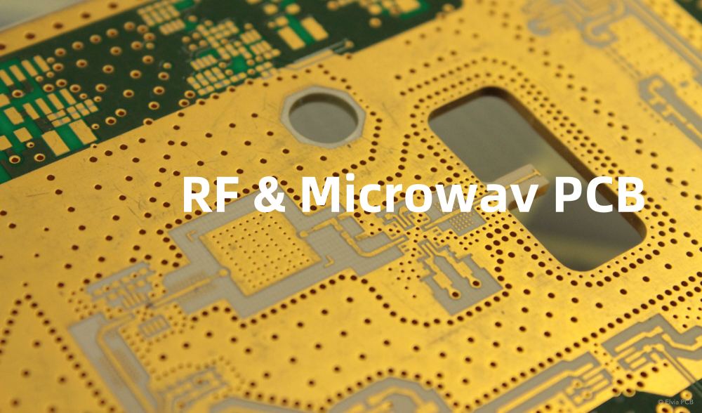
Soldermask via-holes are an essential aspect of printed circuit board (PCB) design, particularly when it comes to chemical Nickel-Gold surface finishes. In this comprehensive article, we will delve into the intricacies of soldermask on via-holes, exploring their importance, the challenges they present, and the best practices for optimizing their performance in PCB manufacturing.
What are via-holes?
Via-holes, or simply vias, are small holes drilled through a PCB to establish electrical connections between different layers of the board. They allow signals and power to be routed vertically, enabling more complex and compact circuit designs. Vias come in various types, such as through-hole vias, blind vias, and buried vias, each serving specific purposes in PCB design.
The role of soldermask in via-holes
Soldermask, also known as solder resist, is a thin layer of polymer applied to the surface of a PCB. Its primary purpose is to protect the copper traces and prevent solder bridges from forming during the soldering process. When it comes to via-holes, soldermask plays a crucial role in ensuring proper electrical insulation and preventing solder from wicking into the via during the assembly process.
Challenges in applying soldermask to via-holes
Soldermask coverage and uniformity
One of the primary challenges in applying soldermask to via-holes is achieving consistent coverage and uniformity. The small size and high aspect ratio of vias can make it difficult for the soldermask to flow evenly into the holes, leading to incomplete coverage or air pockets. This can compromise the electrical insulation properties of the soldermask and potentially lead to reliability issues.
Soldermask adhesion
Another challenge is ensuring proper adhesion of the soldermask to the via walls. Poor adhesion can result in the soldermask lifting or peeling away from the via, exposing the underlying copper and increasing the risk of solder wicking or electrical shorts. Factors such as surface cleanliness, roughness, and compatibility between the soldermask and the via plating material can all impact adhesion.
Thermal expansion and stress
During the PCB manufacturing process, the board undergoes multiple thermal cycles, including soldering and reflow. The difference in thermal expansion coefficients between the soldermask and the via plating material can lead to stress and potential cracking or delamination of the soldermask. This is particularly concerning in the case of chemical Nickel-Gold surface finishes, as the nickel layer can be prone to cracking under thermal stress.
Best practices for soldermask on via-holes
Via design considerations
To minimize challenges with soldermask on via-holes, it is essential to consider via design from the outset. This includes selecting appropriate via sizes and spacing, as well as optimizing the via aspect ratio to facilitate soldermask flow and coverage. Additionally, using via caps or plugs can help prevent solder wicking and improve soldermask adhesion.
Soldermask material selection
Choosing the right soldermask material is crucial for achieving optimal performance on via-holes. Factors to consider include the soldermask’s flow properties, thermal stability, and compatibility with the via plating material. Some advanced soldermask formulations, such as direct imaging (DI) soldermasks, offer improved flow and resolution, enabling better coverage and uniformity on small vias.
Process optimization
Optimizing the soldermask application process can significantly improve the quality and reliability of via-hole coverage. This includes controlling parameters such as soldermask thickness, viscosity, and curing conditions. Employing techniques like vacuum assist or pressure differential can help ensure complete filling of via-holes and eliminate air pockets. Proper cleaning and surface preparation of the PCB prior to soldermask application are also critical for achieving good adhesion.
Quality control and inspection
Implementing stringent quality control measures and inspection procedures is essential for identifying and addressing any issues with soldermask on via-holes. This may involve visual inspection, cross-sectional analysis, or electrical testing to verify soldermask coverage, adhesion, and insulation properties. Utilizing advanced inspection technologies, such as automated optical inspection (AOI) or 3D X-ray, can help detect soldermask defects and ensure consistent quality.

The importance of soldermask via-holes in chemical Nickel-Gold surface finish
Chemical Nickel-Gold surface finish
Chemical Nickel-Gold (ENIG) is a popular surface finish for PCBs, particularly in high-reliability applications. It involves depositing a thin layer of nickel, followed by a thin layer of gold, onto the copper surfaces of the PCB. The nickel layer provides a barrier against copper migration and improves solderability, while the gold layer protects the nickel from oxidation and enhances the surface’s wear resistance.
Soldermask compatibility with ENIG
When applying soldermask to via-holes in PCBs with ENIG surface finish, it is crucial to consider the compatibility between the soldermask and the nickel-gold plating. The soldermask must adhere well to the nickel layer and withstand the thermal stresses associated with the ENIG process. Additionally, the soldermask should not contaminate or degrade the gold surface, which could compromise the solderability and reliability of the PCB.
Challenges specific to ENIG via-holes
One of the main challenges with soldermask on via-holes in ENIG PCBs is the potential for nickel cracking. The nickel layer in ENIG is typically thin and can be prone to cracking under thermal stress, particularly at the via-hole interface. This can lead to soldermask delamination and expose the underlying copper, increasing the risk of solder wicking and electrical shorts.
Another challenge is the potential for gold embrittlement in the via-holes. During the ENIG process, the gold can diffuse into the nickel layer, forming intermetallic compounds that can embrittle the nickel. This can make the via-holes more susceptible to cracking and soldermask delamination, especially during thermal cycling.
Best practices for ENIG via-holes
To mitigate the challenges associated with soldermask on via-holes in ENIG PCBs, several best practices can be employed:
-
Optimize the nickel and gold plating thicknesses to minimize the risk of nickel cracking and gold embrittlement. Thicker nickel layers can provide better stress distribution, while thinner gold layers can reduce the extent of intermetallic formation.
-
Use soldermask materials specifically formulated for compatibility with ENIG surface finishes. These soldermasks should have good adhesion to the nickel layer, high thermal stability, and minimal impact on the gold surface.
-
Employ stress-relief techniques, such as via-in-pad design or the use of filled via-holes, to reduce the stress concentration at the via-hole interface. This can help prevent nickel cracking and soldermask delamination.
-
Implement strict process controls and quality inspections to ensure consistent nickel and gold plating thicknesses, as well as proper soldermask coverage and adhesion in the via-holes.
Frequently Asked Questions (FAQ)
-
Q: What is the purpose of soldermask on via-holes?
A: Soldermask on via-holes serves to provide electrical insulation, prevent solder wicking, and protect the via-hole from contamination during the PCB Assembly process. -
Q: Why is soldermask coverage and uniformity important in via-holes?
A: Consistent soldermask coverage and uniformity in via-holes are crucial for ensuring proper electrical insulation and preventing solder bridges or shorts. Incomplete coverage or air pockets can compromise the reliability of the PCB. -
Q: What challenges are specific to soldermask on via-holes in ENIG PCBs?
A: The main challenges with soldermask on via-holes in ENIG PCBs include the potential for nickel cracking due to thermal stress and gold embrittlement caused by intermetallic formation. These issues can lead to soldermask delamination and expose the underlying copper. -
Q: How can via design considerations help mitigate soldermask challenges?
A: Via design considerations, such as selecting appropriate via sizes and spacing, optimizing via aspect ratios, and using via caps or plugs, can facilitate better soldermask flow, coverage, and adhesion, thereby minimizing challenges associated with soldermask on via-holes. -
Q: What quality control measures are important for soldermask on via-holes?
A: Quality control measures for soldermask on via-holes include visual inspection, cross-sectional analysis, and electrical testing to verify soldermask coverage, adhesion, and insulation properties. Advanced inspection technologies, such as AOI or 3D X-ray, can help detect soldermask defects and ensure consistent quality.
Conclusion
Soldermask on via-holes is a critical aspect of PCB design and manufacturing, particularly in the context of chemical Nickel-Gold surface finishes. Understanding the challenges associated with soldermask coverage, adhesion, and compatibility with ENIG is essential for ensuring the reliability and performance of PCBs.
By implementing best practices in via design, soldermask material selection, process optimization, and quality control, manufacturers can effectively mitigate the risks associated with soldermask on via-holes in ENIG PCBs. This includes optimizing nickel and gold plating thicknesses, using compatible soldermask materials, employing stress-relief techniques, and implementing strict process controls and inspections.
As PCB technology continues to advance, with increasing miniaturization and complexity, the importance of soldermask on via-holes will only grow. By staying informed about the latest developments and best practices in this area, PCB designers and manufacturers can ensure the production of high-quality, reliable boards that meet the evolving demands of the electronics industry.

No responses yet