Introduction to Silkscreen PCB
A printed circuit board (PCB) is a foundational component in virtually all modern electronic devices. PCBs provide the conductive pathways that allow electricity to flow between various components, enabling complex circuits to function as intended. While the copper traces and solder mask are essential for the PCB’s electrical functionality, there is another crucial element that aids in the assembly, testing, and troubleshooting process: the silkscreen.
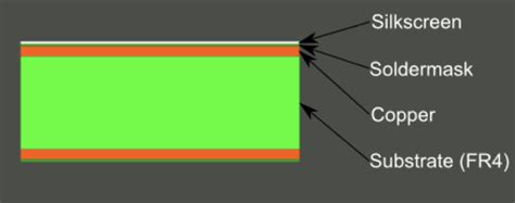
What is a Silkscreen Layer?
The silkscreen layer, also known as the legend or nomenclature layer, is a non-conductive ink layer printed on the surface of a PCB. This layer contains text, symbols, and logos that provide essential information for assembling, testing, and servicing the board. The silkscreen is typically applied using a screen printing process, hence the name “silkscreen.”
The Importance of Silkscreen on PCBs
The silkscreen layer serves several important functions:
-
Component identification: The silkscreen labels components with their reference designators (e.g., R1, C2, U3), making it easier for technicians to locate and identify specific components during assembly, testing, and repair.
-
Orientation markers: Silkscreen can include polarity indicators, pin numbering, and other orientation markers that ensure components are placed correctly on the board.
-
Assembly instructions: The silkscreen may include information such as the board revision number, company logo, or special handling instructions that aid in the assembly process.
-
Debugging and repair: Clear labeling of test points, connectors, and other key features on the silkscreen can greatly simplify debugging and repair tasks.
-
Aesthetics: A well-designed silkscreen can enhance the overall appearance and professionalism of the PCB.
The Silkscreen Printing Process
Screen Printing Basics
The silkscreen printing process involves creating a stencil of the desired artwork and then using that stencil to apply ink to the PCB surface. The stencil, or screen, is typically made of a fine mesh stretched tightly over a frame. The artwork is created on the screen using a photosensitive emulsion that hardens when exposed to light.
Preparing the Artwork
To create the silkscreen artwork, designers use PCB Layout software to generate the silkscreen layer. The artwork must adhere to certain design guidelines to ensure optimal printability:
| Parameter | Recommended Value |
|---|---|
| Minimum line width | 0.15 mm (6 mil) |
| Minimum text size | 1.0 mm (40 mil) |
| Minimum clearance between elements | 0.15 mm (6 mil) |
Applying the Ink
Once the screen is prepared, it is placed over the PCB, and ink is applied using a squeegee. The ink is forced through the open areas of the screen onto the PCB surface. The most common ink colors are white and yellow, as they provide good contrast against the typical green solder mask. After printing, the ink is cured using heat or UV light to ensure durability.

Silkscreen Design Considerations
Component Labeling
One of the primary purposes of the silkscreen is to label components clearly. When designing the silkscreen layer, consider the following:
- Use consistent and clear labeling schemes for reference designators (e.g., R for resistors, C for capacitors, U for ICs)
- Place labels near the component but not so close that they may be obscured by the component itself
- Orient labels to be easily readable without having to rotate the board
Orientation Markers
Proper Component Orientation is critical for a functional PCB. Use the silkscreen to include:
- Polarity indicators for polarized components like electrolytic capacitors and diodes
- Pin 1 markers for ICs and connectors
- Directional arrows or other symbols to indicate the correct orientation of connectors, switches, or other components
Aesthetics and Branding
While the primary purpose of the silkscreen is functional, it also presents an opportunity to enhance the visual appeal and branding of the PCB. Consider incorporating elements such as:
- Company logo or product branding
- Decorative elements or patterns
- Color schemes that complement the overall product design
However, be sure that any aesthetic elements do not compromise the clarity and readability of functional silkscreen elements.

FAQ
1. Is the silkscreen layer necessary for PCB functionality?
No, the silkscreen layer does not affect the electrical functionality of the PCB. However, it is crucial for assembly, testing, and repair processes.
2. Can silkscreen be applied to both sides of the PCB?
Yes, silkscreen can be applied to both the top and bottom surfaces of the PCB, depending on the design requirements.
3. What colors are available for silkscreen ink?
White and yellow are the most common silkscreen ink colors, as they provide good contrast against typical Solder Mask Colors. However, other colors like black, red, or blue may be available depending on the PCB manufacturer.
4. Can silkscreen be removed or modified after printing?
While it is possible to remove silkscreen using abrasive methods or solvents, it is not recommended as it may damage the PCB surface. If modifications are necessary, it is best to update the artwork and reprint the silkscreen.
5. Are there any limitations to the complexity of silkscreen artwork?
The complexity of silkscreen artwork is limited by the resolution of the screen printing process. Fine details or intricate logos may not be reproducible. It is best to consult with the PCB manufacturer for specific artwork guidelines.

Conclusion
The silkscreen layer is a vital component of a well-designed PCB. By providing clear labeling, orientation markers, and assembly instructions, the silkscreen simplifies the manufacturing, testing, and repair processes. A thoughtfully designed silkscreen can also enhance the aesthetics and branding of the final product.
When designing the silkscreen layer, it is essential to adhere to best practices for readability, clarity, and manufacturability. By working closely with the PCB manufacturer and following their artwork guidelines, designers can ensure that the silkscreen effectively serves its intended purposes while also contributing to the overall quality of the PCB.
No responses yet