Understanding the Basics of PCB Layers
Printed Circuit Boards (PCBs) are essential components in modern electronics, forming the backbone of countless devices we use every day. These boards are made up of multiple layers, each serving a specific purpose in the overall functioning of the circuit. In this article, we will focus on the Outer Layer of a PCB, exploring its role, composition, and the various processes involved in its creation.
What is a PCB Layer?
A PCB layer is a thin, flat surface that forms part of the overall structure of a printed circuit board. Each layer serves a specific purpose, such as providing a surface for component placement, facilitating electrical connections, or offering protection from environmental factors. The number of layers in a PCB can vary depending on the complexity of the circuit and the specific requirements of the application.
Types of PCB Layers
PCBs can be classified based on the number of layers they contain. The most common types are:
| PCB Type | Number of Layers |
|---|---|
| Single-layer | 1 |
| Double-layer | 2 |
| Multi-layer | 3 or more |
Single-layer PCBs are the simplest and most cost-effective, while multi-layer PCBs offer more complex routing options and improved performance.
The Outer Layer of a PCB
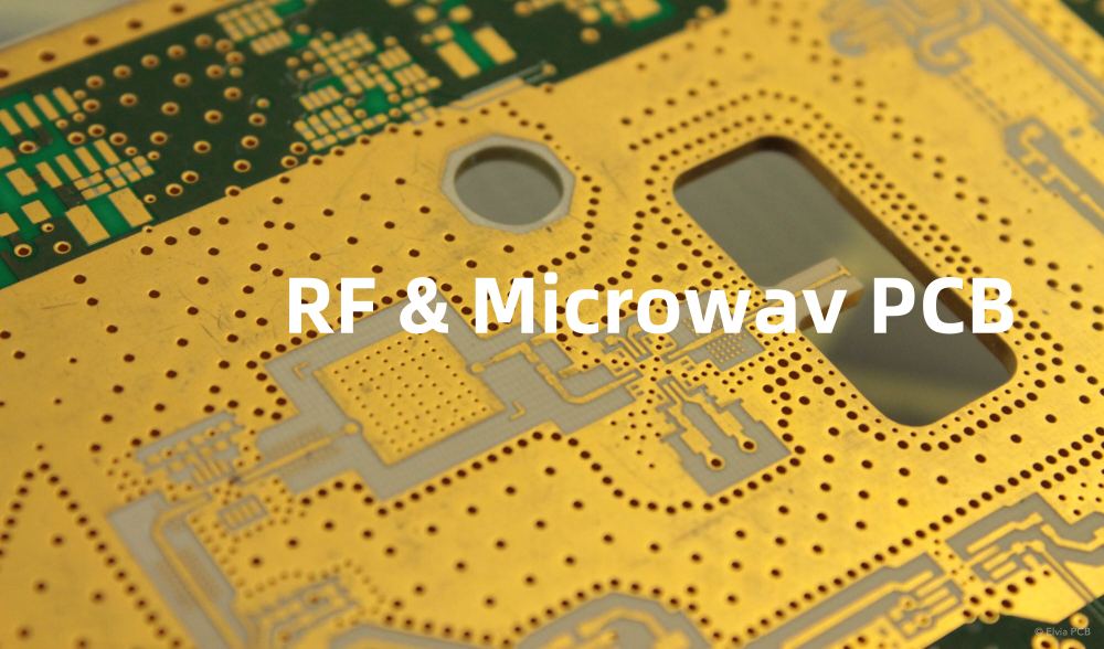
The outer layer of a PCB, also known as the surface layer or top and bottom layers, is the most visible part of the board. It plays a crucial role in the functionality and aesthetics of the PCB.
Functions of the Outer Layer
The outer layer of a PCB serves several key functions:
-
Component Placement: The outer layer provides a surface for mounting electronic components, such as resistors, capacitors, and integrated circuits.
-
Electrical Connections: Conductive traces on the outer layer facilitate electrical connections between components, allowing for the flow of signals and power throughout the circuit.
-
Protection: The outer layer acts as a protective barrier, shielding the internal layers and components from environmental factors such as moisture, dust, and physical damage.
-
Identification: The outer layer often includes labels, logos, and other markings that help identify the PCB and its components, aiding in assembly and troubleshooting processes.
Composition of the Outer Layer
The outer layer of a PCB is typically composed of the following materials:
-
Copper: A thin layer of copper foil is laminated onto the base material, serving as the conductive surface for component placement and electrical connections.
-
Solder Mask: A protective coating, usually green in color, is applied over the copper layer, leaving only the necessary exposed areas for soldering components and creating electrical connections.
-
Silkscreen: A white or colored ink is used to print labels, logos, and other identifying marks on the surface of the PCB.
The Outer Layer Manufacturing Process
Creating the outer layer of a PCB involves several key steps:
1. Copper Foil Lamination
The process begins with the lamination of a thin copper foil onto the base material, which is typically a glass-reinforced epoxy (FR-4). The copper foil is bonded to the base material using heat and pressure, creating a strong and stable foundation for the subsequent steps.
2. Photoresist Application
A photoresist, a light-sensitive material, is applied to the copper surface. This layer will later be used to transfer the desired circuit pattern onto the copper.
3. Exposure and Development
The photoresist-coated PCB is then exposed to UV light through a photomask, which contains the desired circuit pattern. The exposed areas of the photoresist become soluble and are removed during the development process, leaving behind a protective layer in the shape of the circuit pattern.
4. Etching
The exposed copper areas are removed through an etching process, typically using an acidic solution. This leaves behind the desired conductive traces, pads, and other features on the outer layer.
5. Solder Mask Application
A solder mask, usually green in color, is applied over the entire surface of the PCB, covering the copper traces while leaving the necessary areas exposed for soldering components and creating electrical connections. The solder mask provides protection and insulation for the conductive areas.
6. Silkscreen Printing
Finally, a silkscreen layer is applied to the PCB, adding labels, logos, and other identifying marks to the surface. This step aids in the assembly and troubleshooting processes.

Outer Layer Design Considerations
When designing the outer layer of a PCB, several key factors must be taken into account to ensure optimal performance and manufacturability:
1. Component Placement
The placement of components on the outer layer should be carefully considered to minimize the length of conductive traces, reduce signal interference, and facilitate efficient assembly processes.
2. Trace Width and Spacing
The width and spacing of conductive traces on the outer layer must be designed in accordance with the current-carrying requirements and the manufacturing capabilities of the PCB fabricator. Proper trace sizing ensures reliable electrical connections and minimizes the risk of signal integrity issues.
3. Solder Mask Openings
The solder mask openings, or pads, on the outer layer must be designed to accommodate the specific components and soldering techniques used in the assembly process. Proper pad sizing and spacing are crucial for ensuring strong and reliable solder joints.
4. Silkscreen Legibility
The silkscreen layer should be designed with legibility in mind, using clear and concise labeling that is easily readable by both humans and automated assembly equipment. Proper font size, spacing, and contrast are essential for ensuring accurate identification and assembly.
Outer Layer Finishing Options
Once the outer layer of a PCB has been manufactured, several finishing options are available to enhance its performance, durability, and aesthetics:
1. Hot Air Solder Leveling (HASL)
HASL is a common finishing process that involves dipping the PCB in molten solder, then using hot air to remove excess solder and level the surface. This process provides a solderable surface for component attachment and helps protect the copper from oxidation.
2. Electroless Nickel Immersion Gold (ENIG)
ENIG is a high-end finishing option that involves plating the copper surface with a layer of nickel, followed by a thin layer of gold. This process offers excellent solderability, corrosion resistance, and a flat, uniform surface for fine-pitch components.
3. Immersion Silver (IAg)
IAg is a cost-effective alternative to ENIG, offering similar benefits in terms of solderability and flatness. In this process, a thin layer of silver is chemically deposited onto the copper surface, providing protection and enhancing the PCB’s performance.
FAQs
-
Q: What is the purpose of the solder mask on the outer layer of a PCB?
A: The solder mask serves as a protective coating, insulating the copper traces and preventing short circuits. It also helps to prevent solder bridging during the assembly process. -
Q: Can the outer layer of a PCB be used for both component placement and electrical connections?
A: Yes, the outer layer is designed to accommodate both component placement and electrical connections. The exposed copper areas on the outer layer serve as pads for soldering components, while the covered copper traces facilitate electrical connections between components. -
Q: What is the difference between single-layer and multi-layer PCBs?
A: Single-layer PCBs have only one conductive layer, while multi-layer PCBs have three or more conductive layers. Multi-layer PCBs offer more complex routing options and improved performance, but are generally more expensive to manufacture. -
Q: How does the silkscreen layer aid in the assembly and troubleshooting processes?
A: The silkscreen layer provides clear and concise labeling of components, test points, and other important features on the PCB. This labeling helps to ensure accurate assembly and makes it easier to identify and troubleshoot issues during the manufacturing and testing processes. -
Q: What factors should be considered when choosing a finishing option for the outer layer of a PCB?
A: When selecting a finishing option, factors such as the intended application, environmental conditions, component types, and cost should be considered. HASL is a cost-effective choice for general-purpose PCBs, while ENIG and IAg offer superior performance and reliability for more demanding applications.
Conclusion
The outer layer of a PCB is a critical component that plays a vital role in the overall functionality and performance of the board. By understanding the functions, composition, and manufacturing processes involved in creating the outer layer, designers and engineers can make informed decisions when developing PCBs for various applications.
Through careful consideration of design factors such as component placement, trace sizing, and solder mask openings, as well as the selection of appropriate finishing options, the outer layer can be optimized to ensure reliable electrical connections, protection from environmental factors, and ease of assembly and troubleshooting.
As PCB technology continues to advance, the importance of the outer layer will only grow, making it essential for professionals in the electronics industry to stay informed about the latest developments and best practices in PCB design and manufacturing.

No responses yet