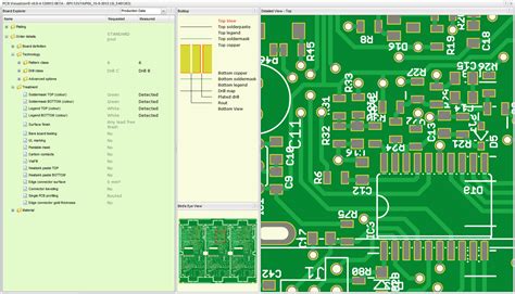
Introduction to PCB Legends
A printed circuit board (PCB) is a fundamental component in modern electronics. It provides a platform for mounting and interconnecting electronic components using conductive traces, pads, and other features. While the design and layout of a PCB are critical for its functionality, another essential aspect is the PCB legend. The PCB legend, also known as silkscreen or overlay, is the layer of text and symbols printed on the surface of the PCB that provides important information for assembly, testing, and maintenance.
Purpose of PCB Legends
The primary purpose of a PCB legend is to make the PCB more user-friendly and easier to understand. It helps identify components, connectors, and test points, which is crucial for efficient assembly and troubleshooting. Some of the key benefits of having a well-designed PCB legend include:
-
Component Identification: The legend can label each component with its reference designator, making it easier to locate and identify them during assembly or repair.
-
Orientation Guidance: Symbols on the legend can indicate the proper orientation of components such as diodes, electrolytic capacitors, and ICs.
-
Connector Labeling: Labels for connectors can specify their type, pinout, and function, helping to prevent incorrect connections.
-
Test Point Identification: The legend can mark test points, making it easier to probe the board during testing and debugging.
-
Branding and Aesthetics: The legend can include company logos, product names, and other branding elements to enhance the visual appeal of the PCB.
Designing a PCB Legend
Legend Placement
When designing a PCB legend, it’s important to consider the placement of the text and symbols. The legend should be readable and unobstructed by components or other features on the board. Here are some guidelines for legend placement:
-
Component Clearance: Ensure that the legend does not interfere with component placement or soldering. Maintain sufficient clearance around components, especially those with tight tolerances.
-
Readability: Place the legend in areas where it is easily readable, typically on the top side of the board. Avoid placing text or symbols too close to the edge of the board or in areas that may be covered by connectors or mounting hardware.
-
Orientation: Orient the text and symbols in a way that is intuitive and easy to read. For example, text should be parallel to the edges of the board or aligned with the component it is labeling.
-
Consistency: Maintain a consistent placement scheme throughout the board. For example, always place reference designators above or below the component, not randomly.
Legend Content
The content of the PCB legend should be clear, concise, and relevant to the assembly and operation of the board. Here are some common elements found in PCB legends:
-
Reference Designators: Each component should be labeled with its reference designator, such as R1 for resistors, C1 for capacitors, and U1 for ICs.
-
Component Values: For passive components like resistors and capacitors, the legend can include the component value, tolerance, and package size.
-
Pin Numbers: For ICs and connectors, pin numbers can be labeled to help identify individual pins during assembly or troubleshooting.
-
Polarity Markers: Polarity-sensitive components such as diodes, electrolytic capacitors, and LEDs should have polarity markers to indicate the correct orientation.
-
Test Points: Test points can be labeled with their function or expected voltage level to aid in debugging.
-
Warnings and Notes: The legend can include warnings or notes about handling, assembly, or operation of the board.
Here’s an example table showing some common legend elements and their purposes:
| Legend Element | Purpose |
|---|---|
| Reference Designator | Identifies individual components |
| Component Value | Specifies the value and package of passive components |
| Pin Number | Labels individual pins of ICs and connectors |
| Polarity Marker | Indicates the correct orientation of polarized components |
| Test Point | Marks points for probing and debugging |
| Warning/Note | Provides important information about handling or operation |
Legend Sizing and Formatting
The size and formatting of the PCB legend should be chosen to ensure readability and clarity. Here are some factors to consider:
-
Text Size: The text size should be large enough to be easily readable, typically at least 0.8mm in height. Smaller text sizes may be used for less critical information or in space-constrained designs.
-
Text Thickness: The thickness of the text should be sufficient to ensure good visibility and durability. A minimum thickness of 0.15mm is recommended.
-
Font: Choose a simple, clear font that is easy to read. Sans-serif fonts like Arial or Helvetica are commonly used.
-
Color: The legend color should contrast well with the PCB substrate color. White legends on green or black substrates are typical, but other colors may be used for aesthetic or functional reasons.
-
Line Width: For symbols and graphics, use a line width that is easily visible and durable. A minimum width of 0.15mm is recommended.
Here’s a table summarizing the recommended sizing and formatting guidelines:
| Parameter | Recommended Value |
|---|---|
| Text Size | ≥ 0.8mm |
| Text Thickness | ≥ 0.15mm |
| Font | Sans-serif (e.g., Arial, Helvetica) |
| Color | High contrast with substrate |
| Line Width | ≥ 0.15mm |
Legend Placement Examples
Here are a few examples of good legend placement practices:
- Component Labeling: Place reference designators and values close to the component, but not so close as to interfere with soldering.
Example:
   C1
0.1µF
  | |
 -----
| o o |
+-----+
- Connector Labeling: Label connectors with their type, function, and pin numbers. Place the labels near the connector, but not so close as to be obscured when the connector is mated.
Example:
 +-------+
 | o o o |
 | o o o |  J1
 | o o o |  USB
 +-------+
- Test Point Labeling: Label test points with their function or expected voltage. Place the labels next to the test point, oriented for easy reading.
Example:
     TP1
    +---+
 o--|VCC|
    +---+
     3.3V

PCB Legend Manufacturing
Once the PCB legend design is complete, it must be manufactured onto the PCB. There are several methods for applying the legend, each with its own advantages and limitations.
Silkscreen Printing
Silkscreen printing is the most common method for applying PCB legends. It involves using a fine mesh screen to deposit ink onto the PCB surface. The screen has a stencil of the legend pattern, allowing the ink to pass through only in the desired areas.
Advantages of silkscreen printing include:
– Cost-effective for large quantities
– Durable and long-lasting
– Can produce fine details and sharp edges
Limitations of silkscreen printing include:
– Requires a separate screen for each legend color
– Limited to a few colors per design
– Minimum line width and spacing limitations
Direct Legend Printing
Direct legend printing uses a specialized inkjet printer to deposit the legend ink directly onto the PCB surface. This method offers more flexibility than silkscreen printing and is well-suited for low-volume or prototype designs.
Advantages of direct legend printing include:
– No tooling or setup costs
– Quick turnaround time
– Can produce full-color graphics and images
Limitations of direct legend printing include:
– Higher cost per unit than silkscreen printing
– Less durable than silkscreen printing
– Limited resolution and line width compared to silkscreen
Laser Marking
Laser marking uses a high-power laser to etch the legend directly onto the PCB surface. This method is well-suited for applications that require high durability or permanence.
Advantages of laser marking include:
– Extremely durable and permanent
– Can produce fine details and small text
– No consumables or tooling required
Limitations of laser marking include:
– Higher cost than other methods
– Limited to a single color (usually black or white)
– Can damage the PCB substrate if not carefully controlled
Here’s a comparison table of the different legend manufacturing methods:
| Method | Cost | Durability | Flexibility | Resolution |
|---|---|---|---|---|
| Silkscreen | Low | High | Limited | Moderate |
| Direct | High | Moderate | High | Low |
| Laser | High | Very High | Limited | High |

Frequently Asked Questions (FAQ)
1. What is the purpose of a PCB legend?
A PCB legend provides important information about the components, connectors, and test points on the board. It helps with assembly, testing, and maintenance by making the board more user-friendly and easier to understand.
2. What should be included in a PCB legend?
A PCB legend typically includes reference designators, component values, pin numbers, polarity markers, test points, and any necessary warnings or notes. The specific content will depend on the complexity and purpose of the board.
3. What are the recommended text size and thickness for a PCB legend?
For good readability and durability, a minimum text size of 0.8mm and a minimum text thickness of 0.15mm are recommended. Smaller sizes may be used in space-constrained designs or for less critical information.
4. What is the most common method for applying a PCB legend?
Silkscreen printing is the most common method for applying PCB legends. It is cost-effective for large quantities and produces durable, long-lasting results with good detail and edge quality.
5. Can a PCB legend be printed in full color?
Yes, direct legend printing using inkjet technology can produce full-color graphics and images on the PCB surface. However, this method is more expensive and less durable than silkscreen printing or laser marking.

Conclusion
A well-designed PCB legend is an essential part of any PCB design. It provides critical information for assembly, testing, and maintenance, making the board more user-friendly and easier to understand. When designing a PCB legend, consider factors such as placement, content, sizing, and formatting to ensure readability and clarity. The legend can be manufactured using various methods, including silkscreen printing, direct printing, and laser marking, each with its own advantages and limitations.
By following best practices for PCB legend design and manufacturing, you can create PCBs that are not only functional but also easy to assemble and maintain. A good legend can save time and reduce errors during production and debugging, ultimately leading to a higher-quality and more reliable product.
No responses yet