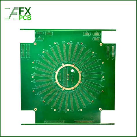
What are PCB Gold Fingers?
PCB gold fingers, also known as edge connectors or contact fingers, are the gold-plated pads or traces located on the edge of a printed circuit board (PCB). These gold-plated contacts are designed to create a reliable electrical connection when inserted into a corresponding socket or connector. Gold fingers are commonly found on various types of PCBs, including computer memory modules, expansion cards, and other pluggable electronic devices.
Benefits of Using Gold for PCB Fingers
Gold is the preferred material for PCB fingers due to its excellent electrical conductivity, corrosion resistance, and durability. Here are some key benefits of using gold for PCB fingers:
-
High Conductivity: Gold is an excellent conductor of electricity, ensuring minimal signal loss and reliable data transmission between the PCB and the mating connector.
-
Corrosion Resistance: Gold is highly resistant to oxidation and corrosion, maintaining its electrical properties even in harsh environments. This makes gold fingers suitable for applications exposed to moisture, chemicals, or extreme temperatures.
-
Durability: Gold is a soft metal, but it is also very malleable and resistant to wear and tear. Gold fingers can withstand numerous insertion and removal cycles without significant degradation, ensuring a long lifespan for the PCB and the mating connector.
-
Low Contact Resistance: Gold has a low contact resistance, which means it requires minimal force to establish a reliable electrical connection. This reduces the risk of intermittent connections and improves signal integrity.
Gold Finger Plating Process
The process of creating gold fingers on a PCB involves several steps:
-
Base Copper Plating: The PCB substrate is first plated with a layer of copper to create the conductive traces and pads.
-
Nickel Plating: A layer of nickel is then plated over the copper to provide a barrier layer and improve the adhesion of the gold plating.
-
Gold Plating: Finally, a layer of gold is plated over the nickel using either an electroplating or an electroless plating process. The gold layer thickness typically ranges from 2 to 30 microinches (0.05 to 0.76 micrometers), depending on the application requirements.
| Layer | Thickness Range | Purpose |
|---|---|---|
| Gold | 2 to 30 microinches (0.05 to 0.76 μm) | Provides excellent conductivity and durability |
| Nickel | 50 to 200 microinches (1.27 to 5.08 μm) | Acts as a barrier layer and improves gold adhesion |
| Copper | 0.5 to 2.8 mils (12.7 to 71.1 μm) | Creates the conductive traces and pads |
Gold Finger Design Considerations
When designing PCBs with gold fingers, several factors should be considered to ensure optimal performance and reliability:
-
Finger Pitch: The pitch, or spacing between the gold fingers, should be carefully designed to match the mating connector. Common pitches include 0.1 inches (2.54 mm), 0.05 inches (1.27 mm), and 0.8 mm.
-
Finger Width: The width of the gold fingers should be sufficient to handle the required current and provide mechanical stability. Wider fingers can carry more current and are less prone to damage during insertion and removal.
-
Finger Length: The length of the gold fingers should be designed to provide adequate contact area with the mating connector. Longer fingers offer more contact surface, reducing contact resistance and improving connection reliability.
-
Chamfered Edges: The edges of the gold fingers should be chamfered or beveled to facilitate smooth insertion into the mating connector and reduce the risk of damage to the fingers or the connector.
-
Solder Mask Clearance: An appropriate solder mask clearance should be maintained around the gold fingers to prevent solder bridging and ensure proper contact with the mating connector.
Applications of PCB Gold Fingers
PCB gold fingers are used in a wide range of electronic applications, including:
Computer Memory Modules
One of the most common applications of PCB gold fingers is in computer memory modules, such as:
- DIMM (Dual In-line Memory Module): Used in desktop computers and laptops for main system memory.
- SO-DIMM (Small Outline DIMM): A smaller version of DIMM used in laptops and compact devices.
- RIMM (Rambus In-line Memory Module): Used in some older systems that utilize Rambus memory technology.
Gold fingers on these memory modules provide a reliable and high-speed connection between the module and the motherboard’s memory slot.
Expansion Cards
Expansion cards, also known as add-on cards or peripheral cards, use PCB gold fingers to connect to a computer’s motherboard via expansion slots. Some common types of expansion cards include:
- Graphics Card (GPU): Used to enhance a computer’s graphics processing capabilities for gaming, video editing, or other visually demanding tasks.
- Sound Card: Provides high-quality audio processing and input/output capabilities.
- Network Interface Card (NIC): Enables a computer to connect to a network, such as Ethernet or Wi-Fi.
- TV Tuner Card: Allows a computer to receive and process television signals.
Gold fingers ensure a reliable connection between the expansion card and the motherboard, enabling high-speed data transfer and stable performance.
Other Applications
PCB gold fingers are also used in various other electronic devices and applications, such as:
- Printed Circuit Board Connectors: Gold fingers are used in board-to-board connectors, backplane connectors, and edge card connectors to establish reliable connections between PCBs or between a PCB and a motherboard.
- Mobile Device Connectors: Some mobile devices, such as smartphones and tablets, use PCBs with gold fingers to connect various components, such as displays, cameras, or battery packs.
- Industrial Control Systems: Gold fingers are used in PCBs for industrial control systems, where reliable connections are critical for proper operation in harsh environments.
- Automotive Electronics: PCBs with gold fingers are used in various automotive electronic systems, such as engine control units, infotainment systems, and driver assistance systems.

PCB Gold Finger Testing and Quality Control
To ensure the reliability and performance of PCB gold fingers, several testing and quality control measures are employed during the manufacturing process:
Visual Inspection
Visual inspection is the first step in quality control, where the gold fingers are examined for any visible defects, such as:
- Scratches, dents, or deformations
- Contamination or foreign material
- Uneven or incomplete gold plating
- Solder mask encroachment or damage
Automated optical inspection (AOI) systems can be used to quickly and accurately detect visual defects on the gold fingers.
Thickness Measurement
The thickness of the gold plating on the PCB fingers is critical for ensuring reliable connections and long-term durability. Various methods can be used to measure the gold thickness, including:
- X-ray Fluorescence (XRF): A non-destructive technique that uses X-rays to measure the thickness and composition of the gold plating.
- Cross-Sectioning: A destructive method where a sample PCB is cut, and the cross-section is examined under a microscope to measure the gold thickness.
- Beta Backscatter: A non-destructive method that uses beta particles to measure the gold thickness without damaging the PCB.
Continuity and Resistance Testing
Electrical continuity and resistance testing are performed to ensure that the gold fingers are properly connected to the PCB traces and that there are no short circuits or open connections. This can be done using:
- Flying Probe Testing: An automated test method that uses movable probes to contact each gold finger and measure its electrical continuity and resistance.
- Bed of Nails Testing: A fixture-based test method where the PCB is pressed against a bed of spring-loaded pins (nails) that contact the gold fingers and measure their electrical properties.
Environmental Testing
To ensure that the PCB gold fingers can withstand the intended operating conditions, various environmental tests may be performed, such as:
- Temperature Cycling: The PCB is subjected to repeated cycles of high and low temperatures to simulate thermal stress and assess the durability of the gold fingers.
- Humidity Testing: The PCB is exposed to high humidity levels to evaluate the resistance of the gold fingers to corrosion and moisture-related failures.
- Vibration and Shock Testing: The PCB is subjected to mechanical vibration and shock to assess the robustness of the gold fingers and their ability to maintain reliable connections under stress.
By conducting these tests and quality control measures, manufacturers can ensure that the PCB gold fingers meet the required specifications and perform reliably in their intended applications.

Frequently Asked Questions (FAQ)
-
Q: What is the purpose of using gold for PCB fingers?
A: Gold is used for PCB fingers because of its excellent electrical conductivity, corrosion resistance, and durability. Gold ensures minimal signal loss, maintains its properties in harsh environments, and can withstand numerous insertion and removal cycles. -
Q: How thick is the gold plating on PCB fingers?
A: The thickness of the gold plating on PCB fingers typically ranges from 2 to 30 microinches (0.05 to 0.76 micrometers), depending on the specific application requirements. -
Q: What is the difference between hard gold and soft gold plating for PCB fingers?
A: Hard gold plating contains a small percentage of cobalt or nickel to increase its hardness and wear resistance, making it suitable for applications with frequent insertions and removals. Soft gold plating, on the other hand, is pure gold and is more malleable, making it better suited for applications with limited insertion cycles or where a low contact force is required. -
Q: Can PCB gold fingers be repaired if damaged?
A: In most cases, damaged PCB gold fingers cannot be easily repaired, as the gold plating is permanently bonded to the underlying nickel and copper layers. Attempting to repair damaged fingers may result in further damage to the PCB or compromised electrical performance. It is generally recommended to replace the entire PCB if the gold fingers are severely damaged. -
Q: Are there any alternatives to using gold for PCB fingers?
A: While gold is the most common and preferred material for PCB fingers, some alternatives include: - Palladium-Nickel Plating: A cheaper alternative that offers good wear resistance and electrical conductivity, but may not match the performance of gold in harsh environments.
- Selective Hard Gold Plating: A process where hard gold is plated only on the contact areas of the fingers, while the rest of the PCB is plated with a cheaper material, such as tin or nickel. This helps reduce costs while maintaining the benefits of hard gold in the critical contact areas.
- Press-Fit Connectors: An alternative connection method that uses a press-fit pin to create a gas-tight connection with the PCB hole, eliminating the need for gold fingers altogether.
However, these alternatives may not provide the same level of performance, reliability, and compatibility as gold fingers in all applications.

Conclusion
PCB gold fingers play a crucial role in establishing reliable electrical connections between PCBs and their mating connectors in various electronic applications. The use of gold plating ensures excellent conductivity, corrosion resistance, and durability, making it the preferred choice for edge connectors.
Designing PCBs with gold fingers requires careful consideration of factors such as finger pitch, width, length, and chamfered edges to ensure optimal performance and compatibility with the intended mating connectors. Proper testing and quality control measures, including visual inspection, thickness measurement, continuity and resistance testing, and environmental testing, are essential to guarantee the reliability and longevity of the gold fingers.
As technology advances and electronic devices become more complex and compact, the importance of reliable and high-performance PCB interconnects will continue to grow. PCB gold fingers will likely remain a key component in ensuring the proper functioning and reliability of these devices in a wide range of applications, from consumer electronics to industrial control systems and beyond.
No responses yet