Introduction to the CD4049 Hex Inverting Buffer
The CD4049, also known as the HEF4049, is a hex inverting buffer integrated circuit that is part of the 4000 series of CMOS logic ICs. This versatile chip contains six independent inverters and operates over a wide voltage range, making it useful for a variety of digital logic applications.
Key features of the CD4049 include:
- Contains six independent inverting buffers
- Wide operating voltage range from 3V to 15V
- High noise immunity
- Low power consumption
- Can drive LEDs, relays, and other loads up to 10mA per output
The CD4049’s combination of multiple inverters, wide voltage range, and high drive capability make it a go-to IC for many hobbyist and commercial logic circuits. Let’s take a closer look at this handy chip and explore some of its common applications.
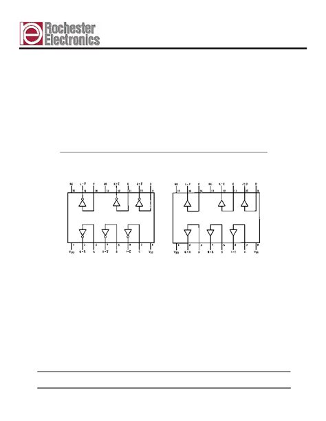
Pinout and Function Table
The CD4049 comes in a 16-pin DIP package with the following pinout:
| Pin | Function |
|---|---|
| 1 | 1A Input |
| 2 | 1Y Output |
| 3 | 2A Input |
| 4 | 2Y Output |
| 5 | 3A Input |
| 6 | 3Y Output |
| 7 | Ground |
| 8 | 4Y Output |
| 9 | 4A Input |
| 10 | 5Y Output |
| 11 | 5A Input |
| 12 | 6Y Output |
| 13 | 6A Input |
| 14 | Not Used |
| 15 | Not Used |
| 16 | VDD |
Each of the six inverters has its own input (nA) and output (nY). All inverters share a common ground (pin 7) and VDD supply (pin 16). Pins 14 and 15 are not connected.
The logic function table is simple – each inverter output is always the opposite state of its input:
| Input | Output |
|---|---|
| Low | High |
| High | Low |
When an input pin is low (connected to ground), the corresponding output will be high (VDD). When the input is high (VDD), the output goes low (ground). This inverting action allows the CD4049 to perform logic negation/NOT operations as well as act as a buffer to condition signals.

Operating Characteristics and Absolute Maximum Ratings
To properly use the CD4049 in circuits, it’s important to understand its operating limits and electrical characteristics. Always consult the manufacturer’s datasheet for a specific part number, but key specifications include:
- Operating voltage range: 3V to 15V
- Maximum supply current: 50mA
- Input voltage range: -0.5V to VDD + 0.5V
- Allowable input current: ±10mA
- Maximum output current per pin: 10mA
- Operating temperature range: -40°C to +85°C
Never exceed the absolute maximum ratings to avoid damaging the IC. The recommended operating conditions for the CD4049 are:
- VDD supply voltage: 5V to 12V
- Input low voltage: 0V to 30% of VDD
- Input high voltage: 70% of VDD to VDD
Under these conditions with a 5V supply, the typical propagation delay is 60ns, power dissipation is 20μW per inverter, and the chip can toggle outputs up to a few MHz.

Driving Loads and Interfacing
One advantage of the CD4049 is its relatively high output drive capability compared to standard logic gates. Each output can sink or source up to 10mA, allowing it to directly drive small loads like LEDs, buzzers, and relay coils.
To drive an LED, connect the cathode to an output pin and the anode to VDD through an appropriate current-limiting resistor. Size the resistor using Ohm’s Law to set the LED current – a typical value is around 1k for a 5V supply.
For inductive loads like relays, include a clamping diode across the coil to protect the IC from voltage spikes when switching off. Connect the diode cathode to VDD and anode to the output pin.
The CD4049’s wide supply range also makes it useful for logic level shifting between 5V and 3.3V systems. By running the chip at 3.3V, it can interface 3.3V logic to 5V circuits without additional components needed.

Application 1: Logic NOT Gates
The most basic use of the CD4049 is as six independent inverters for logic negation. Each inverter performs a NOT operation on its input signal.
For example, to invert three logic signals:
- Connect CD4049 pin 7 to ground and pin 16 to VDD
- Connect signal 1 to pin 1 (1A) and its negated output appears on pin 2 (1Y)
- Connect signal 2 to pin 3 (2A) and its negated output appears on pin 4 (2Y)
- Connect signal 3 to pin 5 (3A) and its negated output appears on pin 6 (3Y)
The remaining three inverters can be used for additional signals or other purposes.
Application 2: Square Wave Oscillator
By connecting an inverter’s output to its input through a resistor/capacitor network, the CD4049 can generate square wave signals for timing or clock purposes.
A simple RC oscillator circuit using one inverter is:
- Connect CD4049 pin 7 to ground and pin 16 to VDD
- Connect a resistor R between the inverter input (pin 1) and output (pin 2)
- Connect a capacitor C between the inverter input and ground
The oscillation frequency f is approximately:
f = 1 / (2.2 × R × C)
Where R is in ohms and C is in farads. For example, with R=100k and C=100pF, the frequency is around 45 kHz. Adjust R and C to set the desired frequency.
The remaining inverters can buffer and output the oscillation signal if higher drive is needed.
Application 3: Delay and Debounce Circuit
An inverter with an RC network can also delay and debounce switch contacts and other noisy digital inputs.
A simple switch debounce circuit is:
- Connect the switch between the inverter input and ground with a pull-up resistor to VDD
- Add a capacitor C in parallel with the switch
- The inverter output is the debounced signal
When the switch closes, the capacitor discharges and prevents contact bounce from reaching the output. An R value of 10k and C of 0.1uF gives a debounce time of around 1ms.
Cascading multiple RC inverter stages increases the total delay time for longer debounce or precise timing applications.
Application 4: Frequency Divider
Since each CD4049 inverter output toggles with every input transition, multiple inverters can divide a clock frequency by powers of two.
To divide a clock signal by 2, 4, 8, or 16:
- Connect the input clock to the first inverter input
- Feed the output of each inverter stage to the input of the next
- The output of the first inverter divides the clock by 2, second by 4, third by 8, etc.
This simple “ripple counter” provides multiple divided-down frequencies synchronized to the input clock.
Application 5: Voltage Level Detector
The CD4049 can sense analog voltage levels by connecting a reference voltage to an input through a resistor divider or potentiometer.
When the input crosses the inverter’s logic threshold (typically around VDD/2), the output switches state. To make a voltage level detector:
- Set up a resistor divider between the analog voltage and ground
- Connect the divider output to an inverter input
- The inverter output indicates if the analog voltage is above/below the threshold
Hysteresis can be added with positive feedback from output to input to prevent oscillation near the threshold.
FAQ
- What is the difference between the CD4049 and the 74HC04 Hex Inverter?
The key differences are that the CD4049 is unbuffered for higher drive capability (10mA per output vs 4mA), has a wider supply voltage range (3-15V vs 2-6V), and comes in a 16-pin package with uncommitted pins vs. 14-pin for the 74HC04. The 74HC04 has faster propagation delay and higher frequency range.
- Can the unused inverters in the CD4049 be left unconnected?
Yes, any unused inputs can be left floating and outputs left open. However, it is good practice to tie unused inputs to ground or VDD to prevent oscillation from picking up noise. Unused outputs can be connected together to increase drive if needed.
- Is the CD4049 static sensitive?
Like most CMOS ICs, the CD4049 can be damaged by electrostatic discharge (ESD). Handle the chip with standard ESD precautions like grounded wrist straps and conductive foam. Unused chips should be kept in conductive storage.
- What happens if the CD4049 inverter input is left floating?
A floating CMOS input can pick up stray noise and cause the output to oscillate or draw high current. Always connect unused inputs to ground or VDD. If an input signal is not always driven, include a pull-up or pull-down resistor to keep the input at a valid logic level.
- Can the CD4049 be used as an anaLog Amplifier?
While the CD4049 inverters can operate in their linear region by using negative feedback, this is not an intended application. Op-amps are a better choice for analog amplification. Using the CD4049 as an amplifier may cause instability, distortion, and noise issues.
Conclusion
The CD4049 hex inverting buffer is a versatile building block for a wide range of digital logic circuits. Its key features of six independent inverters, wide voltage range, high output drive, and low power consumption make it useful for signal conditioning, timing, oscillation, and interfacing applications.
By understanding the CD4049’s pinout, electrical characteristics, and common circuit configurations, a designer can harness the chip’s flexibility to solve many digital logic problems. While not suited for very high speed or analog applications, the CD4049 is a go-to IC for 5V and 3.3V logic designs.
When using the CD4049, remember to operate within its absolute maximum ratings, properly handle unused pins, and include measures like current limiting and clamping diodes to protect the chip and load. With these guidelines in mind, the CD4049 hex inverter can be a valuable addition to any digital designer’s toolkit.
No responses yet