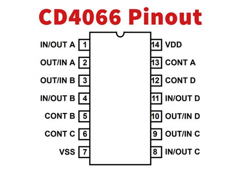
Features of the CD4066
The CD4066 offers several key features that make it an attractive choice for designers:
- Quad Bilateral Switch: The CD4066 contains four independent bilateral switches, allowing for versatile circuit configurations.
- Low On-Resistance: When the switches are closed, they exhibit a low on-resistance, typically around 100 ohms or less, minimizing signal attenuation.
- Wide Supply Voltage Range: The CD4066 can operate with supply voltages ranging from 3V to 15V, making it compatible with various power supply configurations.
- High Switching Speed: The switches in the CD4066 can transition between on and off states quickly, enabling high-frequency operation.
- Low Leakage Current: When the switches are open, the leakage current is extremely low, typically in the range of a few nanoamperes, ensuring minimal signal leakage.
- TTL/CMOS Compatible: The control inputs of the CD4066 are compatible with both TTL and CMOS logic levels, allowing easy interfacing with digital control circuits.
Working Principle of the CD4066
The CD4066 consists of four bilateral switches, each controlled by a separate control input. The working principle of each switch is based on CMOS (Complementary Metal-Oxide-Semiconductor) technology.
Switch Structure
Each switch in the CD4066 is composed of two complementary MOS transistors, an N-channel MOSFET and a P-channel MOSFET. These transistors are connected in parallel, with their gates connected to the control input and their drains and sources connected to the switch terminals.
Switch Operation
The operation of each switch in the CD4066 is controlled by the voltage applied to its control input:
- Switch ON: When a high logic level (typically VDD) is applied to the control input, both the N-channel and P-channel MOSFETs are turned on. This creates a low-resistance path between the switch terminals, allowing the analog signal to pass through with minimal attenuation.
- Switch OFF: When a low logic level (typically VSS or ground) is applied to the control input, both the N-channel and P-channel MOSFETs are turned off. This creates a high-resistance path between the switch terminals, effectively isolating the analog signal.
The use of complementary MOSFETs in the switch structure ensures a low on-resistance and minimal signal distortion when the switch is closed, while providing high isolation when the switch is open.

Applications of the CD4066
The CD4066 finds applications in a wide range of electronic circuits and systems. Some of the common applications include:
1. Analog Signal Switching
The CD4066 is commonly used for switching analog signals, such as audio and video signals. It can be used to route signals between different stages of a circuit or to select between multiple signal sources.
Example: Audio Signal Switching
| Component | Function |
|---|---|
| CD4066 | Switches the audio signal between different audio channels |
| Audio Input | Provides the audio signal to be switched |
| Control | Determines which audio channel is selected |
| Audio Output | Outputs the selected audio signal |
2. Sample and Hold Circuits
The CD4066 can be used in sample and hold circuits, where an analog signal is sampled and held at a specific voltage level for a certain duration. The switch in the CD4066 is used to control the sampling and holding of the signal.
Example: Simple Sample and Hold Circuit
| Component | Function |
|---|---|
| CD4066 | Acts as a switch to control the sampling and holding of the signal |
| Input Signal | The analog signal to be sampled and held |
| Capacitor | Holds the sampled voltage level |
| Control | Determines when the signal is sampled and held |
| Output | The sampled and held voltage level |
3. Multiplexing and Demultiplexing
The CD4066 can be used as a multiplexer or demultiplexer to select one of several analog signals based on digital control inputs. This is useful in applications where multiple signals need to be routed to a single destination or a single signal needs to be distributed to multiple destinations.
Example: 4-to-1 Analog Multiplexer
| Component | Function |
|---|---|
| CD4066 | Acts as switches to select one of the four analog inputs |
| Analog Inputs | The four analog signals to be multiplexed |
| Control Inputs | Binary inputs that determine which analog input is selected |
| Output | The selected analog signal |
4. Voltage-Controlled Resistors
By connecting a resistor in series with a switch in the CD4066, a voltage-controlled resistor can be created. The resistance between the switch terminals can be varied by controlling the voltage applied to the control input.
Example: Voltage-Controlled Attenuator
| Component | Function |
|---|---|
| CD4066 | Acts as a switch to control the attenuation |
| Resistor | Determines the attenuation level when the switch is closed |
| Input Signal | The signal to be attenuated |
| Control | Controls the attenuation by opening or closing the switch |
| Output | The attenuated signal |
5. Chopper Stabilized Amplifiers
The CD4066 can be used in chopper stabilized amplifiers to minimize offset voltage and low-frequency noise. The switches in the CD4066 are used to periodically swap the input and output of the amplifier, effectively canceling out the offset voltage and noise.
Example: Basic Chopper Stabilized Amplifier
| Component | Function |
|---|---|
| CD4066 | Acts as switches to swap the input and output of the amplifier |
| Amplifier | The amplifier to be stabilized |
| Input Signal | The signal to be amplified |
| Control | Generates the chopping frequency to control the switches |
| Output | The amplified and stabilized signal |

Frequently Asked Questions (FAQ)
1. What is the difference between the CD4066 and other analog switches?
The CD4066 is a quad bilateral switch, meaning it contains four independent switches that can conduct current in both directions when closed. It is specifically designed for switching analog signals with low on-resistance and minimal distortion. Other analog switches may have different configurations, such as single or dual switches, and may be optimized for different performance parameters.
2. Can the CD4066 be used for switching digital signals?
While the CD4066 is primarily designed for switching analog signals, it can also be used for switching digital signals. However, it is important to ensure that the digital signal levels are compatible with the supply voltage range of the CD4066 and that the switching speed is sufficient for the desired application.
3. What is the maximum supply voltage that can be used with the CD4066?
The CD4066 can operate with supply voltages ranging from 3V to 15V. It is important not to exceed the maximum supply voltage rating to avoid damaging the device.
4. How fast can the CD4066 switch between the on and off states?
The switching speed of the CD4066 depends on several factors, such as the supply voltage, load capacitance, and the characteristics of the control input signal. Typically, the CD4066 can achieve switching times in the range of a few nanoseconds to a few microseconds.
5. Are there any precautions to be taken when using the CD4066?
When using the CD4066, it is important to consider the maximum ratings of the device, such as the maximum supply voltage, maximum current handling capability, and maximum power dissipation. It is also recommended to use appropriate circuit design techniques, such as proper grounding and shielding, to minimize noise and interference that may affect the performance of the analog signals being switched.

Conclusion
The CD4066 is a versatile quad bilateral switch IC that finds applications in a wide range of electronic circuits and systems. Its key features, including low on-resistance, wide supply voltage range, and high switching speed, make it an attractive choice for switching analog signals with minimal distortion. Understanding the working principle and the various applications of the CD4066 empowers designers to effectively utilize this device in their projects. By considering the specific requirements of the application and following proper design guidelines, the CD4066 can be leveraged to create robust and efficient analog switching solutions.
No responses yet