What is a Digital Buffer?
A digital buffer is an electronic circuit that is used to isolate and amplify a digital signal. It is a crucial component in many digital systems, such as computers, microcontrollers, and digital communication devices. The primary purpose of a digital buffer is to maintain the integrity of a digital signal as it travels through a system, preventing signal degradation and ensuring reliable data transmission.
Types of Digital Buffers
There are several types of digital buffers, each with its own characteristics and applications:
-
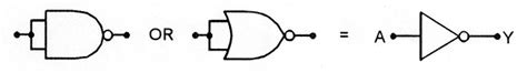
Inverting Buffer: An inverting buffer, also known as a NOT gate, inverts the input signal. If the input is high (1), the output will be low (0), and vice versa.
-
Non-Inverting Buffer: A non-inverting buffer, also known as a unity gain buffer, maintains the same logic level as the input signal. If the input is high (1), the output will also be high (1), and if the input is low (0), the output will be low (0).
-
Tri-State Buffer: A tri-state buffer has three output states: high (1), low (0), and high-impedance (Z). When the enable input is active, the buffer operates as a normal non-inverting buffer. When the enable input is inactive, the buffer’s output goes into a high-impedance state, effectively disconnecting it from the rest of the circuit.
-
Schmitt Trigger Buffer: A Schmitt trigger buffer is a special type of buffer that has hysteresis, which means that it has different threshold voltages for the rising and falling edges of the input signal. This helps to reduce the effects of noise and improve the overall stability of the circuit.
Applications of Digital Buffers
Digital buffers are used in a wide range of applications, including:
-
Signal Conditioning: Digital buffers are often used to condition digital signals, such as cleaning up noisy signals or converting voltage levels between different parts of a system.
-
Fan-Out: When a digital signal needs to drive multiple inputs, a buffer can be used to increase the fan-out capability of the signal source, ensuring that the signal remains strong enough to drive all the connected inputs.
-
Impedance Matching: Digital buffers can be used to match the impedance between different parts of a circuit, preventing signal reflections and ensuring proper signal transmission.
-
Isolation: Buffers can be used to isolate different sections of a digital system, preventing interference and ensuring proper operation.
How Do Digital Buffers Work?
Digital buffers are essentially amplifiers that operate in the digital domain. They take a digital input signal and produce an output signal with the same logic level, but with increased current drive capability.
Basic Operation
The basic operation of a digital buffer can be understood by examining the transfer characteristic of an ideal buffer:
| Input | Output |
|---|---|
| 0 | 0 |
| 1 | 1 |
As shown in the table, when the input is low (0), the output is also low (0), and when the input is high (1), the output is high (1). This is the fundamental behavior of a non-inverting buffer.
Buffer Implementation
Digital buffers are typically implemented using transistors, which are the building blocks of modern electronic circuits. The most common type of transistor used in digital buffers is the MOSFET (Metal-Oxide-Semiconductor Field-Effect Transistor).
A simple non-inverting buffer can be constructed using a single NMOS (N-channel MOSFET) and a single PMOS (P-channel MOSFET) transistor, as shown in the following schematic:
VDD
 |
 |
 +---+
 |   |
 |  PMOS
 |   |
 +---+
   |
   +------ Output
   |
 +---+
 |   |
 |  NMOS
 |   |
 +---+
 |
 |
GND
In this configuration, when the input is low (0), the NMOS transistor is turned off, and the PMOS transistor is turned on, pulling the output high (1). When the input is high (1), the PMOS transistor is turned off, and the NMOS transistor is turned on, pulling the output low (0).
Buffer Characteristics
Digital buffers have several key characteristics that determine their performance and suitability for various applications:
-
Propagation Delay: The propagation delay is the time it takes for a change in the input signal to be reflected at the output. A lower propagation delay means that the buffer can operate at higher frequencies.
-
Rise and Fall Times: The rise time is the time it takes for the output signal to transition from a low state to a high state, while the fall time is the time it takes for the output to transition from a high state to a low state. Faster rise and fall times allow for higher-speed operation.
-
Current Drive Capability: The current drive capability determines how much current the buffer can supply to the load connected to its output. A higher current drive capability allows the buffer to drive more inputs or larger loads.
-
Power Consumption: The power consumption of a buffer is determined by factors such as its supply voltage, operating frequency, and load conditions. Lower power consumption is desirable for battery-powered devices and systems with tight power budgets.

Types of Digital Buffer ICs
There are many different types of digital buffer ICs available, each with its own features and benefits. Some of the most common types include:
74HC125 – Quad Tri-State Buffer
The 74HC125 is a quad tri-state buffer IC that features four independent buffers in a single package. Each buffer has a separate enable input, allowing individual control of the output state. The 74HC125 is widely used in applications such as bus interfacing, data transmission, and signal isolation.
74HCT244 – Octal Non-Inverting Buffer
The 74HCT244 is an octal non-inverting buffer IC that contains eight independent buffers. It is designed for use in high-speed applications and features a high current drive capability, making it suitable for driving large loads or multiple inputs.
74LVC07A – Hex Buffer with Open-Drain Outputs
The 74LVC07A is a hex buffer IC with open-drain outputs, which means that the outputs can be connected together to perform wired-AND operations. This feature makes the 74LVC07A useful in applications such as I2C bus interfacing and open-collector bus systems.
SN74LVC1G07 – Single Buffer with Open-Drain Output
The SN74LVC1G07 is a single buffer IC with an open-drain output, designed for low-voltage, high-speed applications. Its small package size and low power consumption make it ideal for use in portable and battery-powered devices.

Designing with Digital Buffers
When designing with digital buffers, there are several factors to consider to ensure optimal performance and reliability:
-
Signal Integrity: To maintain signal integrity, it is important to minimize the distance between the buffer and the load, and to use proper termination techniques to prevent signal reflections.
-
Power Supply Decoupling: Digital buffers require a clean and stable power supply to operate correctly. Adequate power supply decoupling, using capacitors connected close to the buffer’s supply pins, helps to reduce noise and ensure proper operation.
-
Input and Output Characteristics: When selecting a digital buffer, it is important to consider the input and output characteristics, such as the input voltage range, output voltage swing, and current drive capability, to ensure compatibility with the rest of the system.
-
Timing Considerations: In high-speed applications, timing considerations such as propagation delay, rise and fall times, and skew between different buffers become critical. Careful design and layout techniques, such as matched trace lengths and proper signal routing, can help to minimize these issues.

Frequently Asked Questions (FAQ)
-
What is the difference between a digital buffer and an analog buffer?
A digital buffer operates on digital signals, which have discrete voltage levels representing logical states (0 and 1). An analog buffer, on the other hand, operates on continuous, time-varying signals and is designed to maintain the shape and amplitude of the input signal. -
Can a digital buffer be used to convert voltage levels?
Yes, digital buffers can be used to convert voltage levels between different parts of a system. For example, a buffer with a 5V input voltage range and a 3.3V output voltage range can be used to interface a 5V logic circuit with a 3.3V logic circuit. -
What is the purpose of a tri-state buffer?
A tri-state buffer has three output states: high (1), low (0), and high-impedance (Z). The high-impedance state allows the buffer to disconnect its output from the rest of the circuit, which is useful in applications such as bus interfacing, where multiple devices share the same bus. -
How do I select the right digital buffer for my application?
When selecting a digital buffer, consider factors such as the required input and output voltage levels, current drive capability, speed (propagation delay and rise/fall times), power consumption, and package size. Also, ensure that the buffer is compatible with the rest of your system and meets any specific application requirements. -
What is the role of power supply decoupling in digital buffer circuits?
Power supply decoupling is the practice of connecting capacitors close to the supply pins of digital buffers to provide a low-impedance path for high-frequency noise and transients. This helps to ensure a clean and stable power supply, which is essential for proper operation of the buffer and the overall system.
In conclusion, digital buffers are essential components in modern electronic systems, providing signal isolation, amplification, and conditioning. By understanding the various types of buffers, their characteristics, and design considerations, engineers can effectively incorporate these versatile devices into their designs to ensure reliable and efficient digital signal transmission.
No responses yet