Introduction to the IC 4060 Chip
The IC 4060, also known as the CD4060 or MC14060, is a 14-stage ripple carry binary counter and oscillator integrated circuit. It is part of the 4000 series of CMOS logic chips. The IC 4060 is commonly used for generating timing delays, clock signals, and frequency division in electronic circuits and projects.
This versatile chip features an on-board oscillator that can be controlled by an external resistor and capacitor, allowing designers to set the oscillation frequency according to their requirements. The IC 4060’s ripple counter can divide the oscillator frequency by factors of 2^n, where n ranges from 1 to 14.
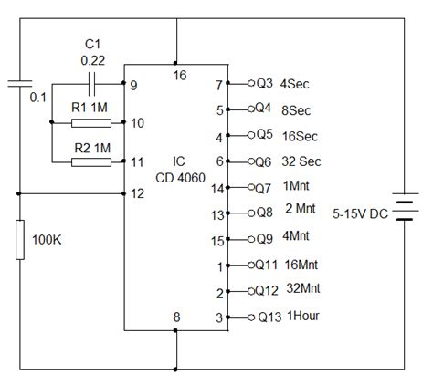
IC 4060 Pinout Diagram
To effectively use the IC 4060 in your projects, it is essential to understand its pinout and the function of each pin. The following table provides an overview of the IC 4060 pinout:
| Pin Number | Pin Name | Description |
|---|---|---|
| 1 | Q13 | Counter output (divide by 8192) |
| 2 | Q12 | Counter output (divide by 4096) |
| 3 | Q11 | Counter output (divide by 2048) |
| 4 | Q5 | Counter output (divide by 32) |
| 5 | Q4 | Counter output (divide by 16) |
| 6 | Q6 | Counter output (divide by 64) |
| 7 | Q3 | Counter output (divide by 8) |
| 8 | GND | Ground |
| 9 | Q0 | Counter output (divide by 1, same as input) |
| 10 | CLK IN/OUT | Clock input/output |
| 11 | RST | Reset input (active high) |
| 12 | Q8 | Counter output (divide by 256) |
| 13 | Q9 | Counter output (divide by 512) |
| 14 | Q10 | Counter output (divide by 1024) |
| 15 | Q14 | Counter output (divide by 16384) |
| 16 | VDD | Positive supply voltage (3V to 15V) |

Detailed Pin Functions
Power Supply Pins
VDD (Pin 16)
The VDD pin is the positive supply voltage input for the IC 4060. It should be connected to a stable DC voltage source ranging from 3V to 15V, depending on the specific requirements of your circuit. It is important to ensure that the supply voltage is within the recommended range to avoid damaging the chip or causing unexpected behavior.
GND (Pin 8)
The GND pin is the ground or negative supply voltage connection for the IC 4060. It should be connected to the common ground of your circuit. Proper grounding is crucial for the stable operation of the chip and helps to minimize noise and interference.
Oscillator Pins
CLK IN/OUT (Pin 10)
The CLK IN/OUT pin serves as both the input and output for the on-board oscillator. When using an external clock source, connect the clock signal to this pin. If using the internal oscillator, this pin will output the oscillator frequency, which can be used as a reference or connected to other parts of your circuit.
To set up the internal oscillator, connect a resistor (R) between the CLK IN/OUT pin and VDD, and a capacitor (C) between the CLK IN/OUT pin and GND. The oscillation frequency (fosc) can be approximated using the following formula:
fosc ≈ 1 / (2.3 × R × C)
Choose the appropriate values for R and C to achieve the desired oscillation frequency.
Reset Pin
RST (Pin 11)
The RST pin is an active-high reset input for the IC 4060. When this pin is held high (connected to VDD), the counter is reset to its initial state, and all outputs are set to low. To enable normal operation, the RST pin should be connected to GND or left unconnected, as it has an internal pull-down resistor.
Counter Output Pins
The IC 4060 features 14 counter output pins, each providing a frequency-divided version of the input clock signal. The division factors range from 2^0 (1) to 2^13 (8192), allowing you to generate various frequencies from a single clock source.
Q0 (Pin 9)
The Q0 output provides the same frequency as the input clock signal, without any frequency division.
Q3 (Pin 7)
The Q3 output divides the input clock frequency by 8 (2^3).
Q4 (Pin 5)
The Q4 output divides the input clock frequency by 16 (2^4).
Q5 (Pin 4)
The Q5 output divides the input clock frequency by 32 (2^5).
Q6 (Pin 6)
The Q6 output divides the input clock frequency by 64 (2^6).
Q8 (Pin 12)
The Q8 output divides the input clock frequency by 256 (2^8).
Q9 (Pin 13)
The Q9 output divides the input clock frequency by 512 (2^9).
Q10 (Pin 14)
The Q10 output divides the input clock frequency by 1024 (2^10).
Q11 (Pin 3)
The Q11 output divides the input clock frequency by 2048 (2^11).
Q12 (Pin 2)
The Q12 output divides the input clock frequency by 4096 (2^12).
Q13 (Pin 1)
The Q13 output divides the input clock frequency by 8192 (2^13).
Q14 (Pin 15)
The Q14 output divides the input clock frequency by 16384 (2^14).

Typical Applications of the IC 4060
The IC 4060 finds applications in various electronic projects and circuits, including:
-
Frequency division: The IC 4060 can be used to divide a high-frequency clock signal into lower frequencies, making it suitable for generating timing signals or clock pulses for different parts of a circuit.
-
Timers and delay generators: By using the IC 4060’s oscillator and counter outputs, you can create programmable timers and delay generators. The duration of the timer or delay can be adjusted by selecting the appropriate counter output and oscillator frequency.
-
PWM generation: The IC 4060 can be used to generate PWM (Pulse Width Modulation) signals by combining the outputs of different counter stages. PWM signals are useful for controlling the brightness of LEDs, the speed of motors, or the power delivered to a load.
-
Sequencers and state machines: The counter outputs of the IC 4060 can be used to create sequencers or state machines. By decoding the counter outputs using logic gates or a multiplexer, you can generate a sequence of signals or control the state of your circuit based on the counter value.
-
Frequency synthesis: The IC 4060 can be used as part of a frequency synthesis circuit, where the desired output frequency is generated by combining and dividing the outputs of multiple 4060 chips or by using the 4060 in conjunction with other frequency synthesis techniques, such as Phase-Locked Loops (PLLs).

Example Circuit: Simple LED Blinker
To demonstrate the usage of the IC 4060, let’s create a simple LED blinker circuit that flashes an LED at a rate of approximately 1 Hz.
Components required:
– IC 4060
– LED
– 220Ω resistor
– 1MΩ resistor
– 100nF capacitor
– Breadboard and jumper wires
Circuit diagram:
        IC 4060
       _____
 VDD -|     |- GND
      |     |
      |  10 |-- R1 (1MΩ) -- VDD
      |     |
      |     |-- C1 (100nF) -- GND
      |     |
      |  7  |-- LED -- 220Ω -- GND
      |_____|
Steps:
1. Connect the VDD (pin 16) of the IC 4060 to the positive supply voltage (e.g., 5V).
2. Connect the GND (pin 8) of the IC 4060 to the ground of your circuit.
3. Connect a 1MΩ resistor (R1) between the CLK IN/OUT (pin 10) and VDD.
4. Connect a 100nF capacitor (C1) between the CLK IN/OUT (pin 10) and GND.
5. Connect the anode of the LED to the Q3 output (pin 7) of the IC 4060.
6. Connect a 220Ω resistor between the cathode of the LED and GND.
In this circuit, the IC 4060’s internal oscillator is set up using R1 and C1 to generate a frequency of approximately 8 Hz. The Q3 output divides this frequency by 8, resulting in a 1 Hz signal that blinks the LED.
You can experiment with different counter outputs or oscillator frequencies to achieve different blinking rates or create more complex patterns.
Frequently Asked Questions (FAQ)
1. What is the maximum supply voltage for the IC 4060?
The maximum supply voltage for the IC 4060 is 15V. It is essential to keep the supply voltage within the specified range (3V to 15V) to ensure proper operation and avoid damaging the chip.
2. Can I use the IC 4060 with a crystal oscillator?
Yes, you can use the IC 4060 with a crystal oscillator. To do this, connect the crystal and the required load capacitors between the CLK IN/OUT (pin 10) and GND (pin 8) of the IC 4060. Consult the crystal oscillator’s datasheet for the recommended load capacitance values.
3. How do I calculate the oscillator frequency for the IC 4060?
The oscillator frequency (fosc) for the IC 4060 can be approximated using the formula: fosc ≈ 1 / (2.3 × R × C), where R is the resistance connected between CLK IN/OUT and VDD, and C is the capacitance connected between CLK IN/OUT and GND. Choose appropriate values for R and C to achieve the desired oscillation frequency.
4. What is the difference between the IC 4060 and the IC 4017?
While both the IC 4060 and the IC 4017 are counter ICs, they have different functionalities. The IC 4060 is a 14-stage ripple carry binary counter with an on-board oscillator, whereas the IC 4017 is a decade counter with 10 decoded outputs. The IC 4060 is primarily used for frequency division and generating timing signals, while the IC 4017 is used for sequencing and controlling up to 10 outputs in a predetermined order.
5. Can I cascade multiple IC 4060 chips to achieve higher frequency division ratios?
Yes, you can cascade multiple IC 4060 chips to achieve higher frequency division ratios. To do this, connect the Q14 output (pin 15) of the first IC 4060 to the CLK IN/OUT (pin 10) of the second IC 4060. This way, the second IC 4060 will divide the already divided frequency from the first chip, resulting in even higher division ratios. You can continue cascading more IC 4060 chips in the same manner to achieve the desired division ratio.
Conclusion
The IC 4060 is a versatile and widely used counter and oscillator chip that finds applications in various electronic projects and circuits. With its on-board oscillator and 14-stage ripple carry binary counter, the IC 4060 offers an easy way to generate timing signals, frequency division, and control sequences.
By understanding the pinout and functions of each pin, you can effectively integrate the IC 4060 into your designs and harness its capabilities. Whether you are creating simple LED blinkers, complex timing circuits, or frequency synthesis systems, the IC 4060 provides a reliable and efficient solution.
As you explore the world of electronics and embark on new projects, keep the IC 4060 in mind as a valuable tool in your arsenal. Experiment with different oscillator frequencies, counter outputs, and cascading configurations to unleash the full potential of this remarkable chip. Happy designing and innovating!
No responses yet