Introduction to Printed Circuit Boards
Printed Wiring Boards (PWBs), also known as Printed Circuit Boards (PCBs), are essential components in modern electronic devices. They provide a platform for mounting and connecting electronic components, enabling the creation of complex circuits in a compact and efficient manner. In this comprehensive article, we will explore the fundamentals of PWBs, their manufacturing process, design considerations, and various applications.
What is a Printed Wiring Board?
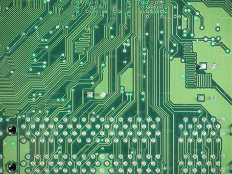
A Printed Wiring Board is a flat insulating substrate made of materials such as fiberglass, epoxy resin, or composite materials. It consists of conductive pathways, known as traces or tracks, which are etched or printed onto the substrate to interconnect electronic components. PWBs provide mechanical support and electrical connectivity for components such as integrated circuits (ICs), resistors, capacitors, and connectors.
Advantages of Printed Wiring Boards
PWBs offer several advantages over traditional point-to-point wiring methods:
- Compact size: PWBs allow for high-density component placement, resulting in smaller and more compact electronic devices.
- Reliability: The use of PWBs reduces wiring errors and improves the overall reliability of electronic circuits.
- Mass production: PWBs enable automated assembly processes, making mass production of electronic devices more efficient and cost-effective.
- Reproducibility: PWB designs can be easily replicated, ensuring consistency and uniformity across multiple production runs.
PWB Manufacturing Process
The manufacturing process of PWBs involves several critical steps to ensure high-quality and reliable boards. Let’s explore each step in detail.
1. PCB Design and Layout
The first step in PWB manufacturing is the design and layout of the circuit. This involves creating a schematic diagram that represents the electrical connections between components. The schematic is then translated into a physical layout using specialized PCB design software. The layout determines the placement of components, routing of traces, and the overall dimensions of the board.
2. PCB Fabrication
Once the PCB design is finalized, the fabrication process begins. The most common method for PCB fabrication is the subtractive process, which involves the following steps:
a. Substrate Preparation
The substrate material, typically a copper-clad laminate, is cut to the desired size and shape. The copper layer is cleaned and prepared for the subsequent steps.
b. Applying Photoresist
A photoresist layer is applied to the copper surface of the substrate. Photoresist is a light-sensitive material that hardens when exposed to ultraviolet (UV) light.
c. Exposure and Development
The PCB layout is transferred onto the photoresist layer using a photomask and UV light exposure. The exposed areas of the photoresist harden, while the unexposed areas remain soluble.
d. Etching
The board is then subjected to an etching process, where the unexposed areas of the photoresist are removed, exposing the underlying copper. The exposed copper is chemically etched away, leaving only the desired conductive tracks.
e. Photoresist Removal
After etching, the remaining photoresist is removed, revealing the final copper pattern on the substrate.
f. Drilling and Plating
Holes are drilled in the board for through-hole components and vias. The holes are then plated with copper to establish electrical connectivity between layers.
g. Solder Mask and Silkscreen
A solder mask layer is applied to the board to protect the copper tracks and prevent solder bridging. A silkscreen layer is added to provide component labels and markings.
3. PCB Assembly
Once the PCB is fabricated, the components are mounted onto the board. There are two main methods for PCB assembly:
a. Through-Hole Assembly (THA)
In through-hole assembly, components with long leads are inserted into the drilled holes on the PWB. The leads are then soldered to the copper pads on the opposite side of the board.
b. Surface Mount Assembly (SMA)
Surface mount assembly involves placing components directly onto the surface of the PWB. The components have small metal pads or leads that are soldered to the corresponding pads on the board.
4. Testing and Inspection
After assembly, the PWB undergoes rigorous testing and inspection to ensure proper functionality and quality. Various tests, such as:
- Visual inspection
- Automated Optical Inspection (AOI)
- In-Circuit Testing (ICT)
- Functional testing
These tests help identify any manufacturing defects, short circuits, or open connections.

PWB Design Considerations
Designing a PWB involves several key considerations to ensure optimal performance, reliability, and manufacturability. Some important design aspects include:
1. Component Placement
Proper component placement is crucial for achieving a compact and efficient board layout. Considerations such as component size, thermal management, and signal integrity should be taken into account.
2. Trace Routing
Trace routing involves creating the conductive paths that connect components on the PWB. Factors such as trace width, spacing, and impedance matching should be considered to minimize signal interference and ensure reliable signal transmission.
3. Grounding and Shielding
Proper grounding and shielding techniques are essential for reducing electromagnetic interference (EMI) and ensuring the stability of sensitive circuits. Ground planes, power planes, and shielding enclosures are commonly used techniques.
4. Thermal Management
Managing heat dissipation is critical for the long-term reliability of electronic components. PWB designers should consider factors such as component placement, copper area, and the use of thermal vias to efficiently dissipate heat.
5. Manufacturing Constraints
PWB designs must adhere to manufacturing constraints to ensure producibility and yield. Considerations such as minimum trace width, spacing, and hole sizes should be taken into account based on the capabilities of the manufacturing process.

PWB Applications
PWBs find applications in a wide range of industries and electronic devices. Some common applications include:
- Consumer Electronics: Smartphones, tablets, laptops, televisions, and gaming consoles.
- Automotive Electronics: Engine control units, infotainment systems, and advanced driver assistance systems (ADAS).
- Medical Devices: Diagnostic equipment, monitoring systems, and implantable devices.
- Industrial Automation: Control systems, sensors, and data acquisition modules.
- Aerospace and Defense: Avionics, radar systems, and communication equipment.

Future Trends in PWB Technology
The field of PWB technology is continuously evolving to meet the demands of advancing electronic systems. Some notable trends include:
- Miniaturization: The trend towards smaller and more compact electronic devices drives the need for high-density interconnect (HDI) PCBs with finer pitch and smaller component sizes.
- Flexible and Stretchable PWBs: Flexible and stretchable PWBs are gaining popularity for applications that require conformable and wearable electronics.
- 3D Printing: Additive manufacturing techniques, such as 3D printing, are being explored for rapid prototyping and customization of PWBs.
- Embedded Components: The integration of passive components, such as resistors and capacitors, directly into the PWB substrate is becoming more common to save space and improve performance.
- High-Speed and High-Frequency Designs: As data transmission rates increase, PWB designs need to accommodate high-speed and high-frequency signals while minimizing signal integrity issues.
Frequently Asked Questions (FAQ)
-
What is the difference between a PWB and a PCB?
A PWB (Printed Wiring Board) and a PCB (Printed Circuit Board) are essentially the same thing. The terms are often used interchangeably in the electronics industry. -
What materials are commonly used for PWB substrates?
Common materials used for PWB substrates include: - FR-4: A composite material made of fiberglass and epoxy resin, widely used for general-purpose applications.
- Polyimide: A high-temperature resistant material used for flexible PWBs and applications requiring high reliability.
-
Ceramic: Used for high-frequency and high-power applications due to its excellent thermal and dielectric properties.
-
What is the purpose of a solder mask on a PWB?
A solder mask is a protective layer applied to the PWB surface to prevent solder bridging between adjacent pads or tracks. It also provides insulation and protection against environmental factors. -
How are components mounted onto a PWB?
Components can be mounted onto a PWB using two main methods: - Through-hole assembly (THA): Components with long leads are inserted into drilled holes and soldered to the pads on the opposite side of the board.
-
Surface mount assembly (SMA): Components with small metal pads or leads are placed directly onto the surface of the PWB and soldered to the corresponding pads.
-
What is the role of testing and inspection in PWB manufacturing?
Testing and inspection are critical steps in PWB manufacturing to ensure the quality and functionality of the finished boards. Various tests, such as visual inspection, automated optical inspection (AOI), in-circuit testing (ICT), and functional testing, are performed to identify any defects, short circuits, or open connections.
Conclusion
Printed Wiring Boards (PWBs) play a crucial role in the world of electronics, providing a reliable and efficient means of interconnecting electronic components. Understanding the fundamentals of PWBs, including their manufacturing process, design considerations, and applications, is essential for anyone involved in the development or production of electronic devices.
As technology continues to advance, PWB technology will evolve to meet the demands of increasingly complex and miniaturized electronic systems. Trends such as miniaturization, flexible and stretchable PWBs, 3D printing, embedded components, and high-speed designs will shape the future of PWB manufacturing.
By staying informed about the latest developments and best practices in PWB technology, engineers and designers can create innovative and reliable electronic products that meet the needs of today’s rapidly evolving market.
No responses yet