Introduction
Printed Circuit Board (PCB) soldering is a crucial process in the manufacturing of electronic devices. It involves the attachment of electronic components to the PCB using molten solder. However, various defects can occur during the soldering process, leading to malfunctions, short circuits, or complete failure of the electronic device. In this article, we will discuss 9 common PCB Soldering Defects and their solutions.
What is PCB Soldering?
PCB soldering is the process of joining electronic components to a printed circuit board using molten solder. The solder is a metal alloy that melts at a relatively low temperature, allowing it to flow and create a strong bond between the component leads and the PCB pads. Proper soldering ensures a reliable electrical connection and mechanical stability of the components on the PCB.

Why is Proper PCB Soldering Important?
Proper PCB soldering is essential for several reasons:
-
Electrical Conductivity: A well-soldered joint ensures a low-resistance electrical connection between the component and the PCB, allowing signals and power to flow efficiently.
-
Mechanical Stability: Soldering provides mechanical support to the components, preventing them from moving or detaching from the PCB during handling or operation.
-
Reliability: Properly soldered joints are less likely to fail over time due to factors such as vibration, thermal stress, or corrosion.
-
Product Quality: Poor soldering can lead to malfunctions, short circuits, or complete failure of the electronic device, compromising its quality and reliability.

Common PCB Soldering Defects
Here are 9 common PCB soldering defects and their solutions:
1. Bridging
Bridging occurs when solder inadvertently connects two or more pads or traces that should not be connected. This can cause short circuits and lead to malfunctions or damage to the electronic device.
Causes:
- Excessive solder
- Improper soldering technique
- Incorrect component placement
- Contamination on the PCB or component leads
Solutions:
- Use the appropriate amount of solder
- Ensure proper soldering technique and temperature control
- Double-check component placement before soldering
- Clean the PCB and component leads before soldering
2. Cold Joints
Cold joints occur when the solder fails to melt and flow properly, resulting in a weak and unreliable connection. The solder joint appears dull, grainy, or cracked.
Causes:
- Insufficient heat during soldering
- Improper flux usage
- Contamination on the PCB or component leads
- Incorrect soldering iron tip size or shape
Solutions:
- Ensure the soldering iron is at the correct temperature
- Use appropriate flux and apply it correctly
- Clean the PCB and component leads before soldering
- Select the appropriate soldering iron tip for the job
3. Insufficient Solder
Insufficient solder refers to a lack of solder in the joint, resulting in a weak or incomplete connection. This can lead to intermittent failures or complete disconnection of the component.
Causes:
- Applying too little solder
- Incorrect soldering technique
- Contamination preventing solder flow
- Incorrect pad or lead design
Solutions:
- Apply the appropriate amount of solder
- Ensure proper soldering technique
- Clean the PCB and component leads before soldering
- Verify pad and lead designs are suitable for soldering
4. Excessive Solder
Excessive solder occurs when too much solder is applied to the joint, potentially causing bridging, short circuits, or impeding the placement of nearby components.
Causes:
- Applying too much solder
- Incorrect soldering technique
- Using a soldering iron tip that is too large
- Insufficient heat, causing the solder to pile up
Solutions:
- Apply the appropriate amount of solder
- Ensure proper soldering technique
- Select the appropriate soldering iron tip size
- Maintain the correct soldering iron temperature
5. Lifted Pads
Lifted pads occur when the copper pad on the PCB separates from the board during soldering or component removal. This can result in an unreliable or broken connection.
Causes:
- Excessive heat during soldering or desoldering
- Mechanical stress during component removal
- Poor PCB manufacturing quality
- Incorrect pad design or copper thickness
Solutions:
- Control the soldering iron temperature and duration
- Use proper desoldering techniques and tools
- Ensure PCB manufacturing quality meets standards
- Verify pad designs are suitable for the application
6. Tombstoning
Tombstoning, also known as drawbridging, occurs when a surface-mount component stands up on one end due to uneven heating or surface tension during reflow soldering.
Causes:
- Uneven heating of the component pads
- Incorrect pad design or placement
- Insufficient or excessive solder paste
- Incorrect reflow soldering profile
Solutions:
- Ensure even heating of the component pads
- Verify pad designs and placement are correct
- Apply the appropriate amount of solder paste
- Optimize the reflow soldering profile
7. Solder Balls
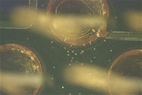
Solder balls are small, spherical balls of solder that can cause short circuits or interfere with the placement of nearby components.
Causes:
- Excessive solder paste
- Incorrect reflow soldering profile
- Contamination on the PCB or component leads
- Incorrect paste stencil design or thickness
Solutions:
- Apply the appropriate amount of solder paste
- Optimize the reflow soldering profile
- Clean the PCB and component leads before soldering
- Verify paste stencil design and thickness are correct
8. Flux Residue
Flux residue is the remnants of the flux used during soldering that can cause corrosion, insulation resistance issues, or interfere with the operation of the electronic device.
Causes:
- Using non-clean flux without proper cleaning
- Insufficient cleaning after soldering
- Incorrect flux selection for the application
- Excessive flux application
Solutions:
- Use no-clean flux when possible
- Ensure proper cleaning of the PCB after soldering
- Select the appropriate flux for the application
- Apply the correct amount of flux
9. Whiskers
Whiskers are thin, metallic filaments that grow from the surface of the solder joint over time. They can cause short circuits or intermittent connections.
Causes:
- Use of lead-free solder alloys
- Mechanical stress on the solder joint
- Contamination or impurities in the solder
- Incorrect storage conditions
Solutions:
- Use solder alloys with a lower risk of whisker formation
- Minimize mechanical stress on the solder joints
- Ensure the use of high-quality, contaminant-free solder
- Store PCBs and components in a controlled environment

Visual Guide to PCB Soldering Defects
| Defect | Appearance | Causes | Solutions |
|---|---|---|---|
| Bridging | – Excessive solder – Improper soldering technique – Incorrect component placement – Contamination |
– Use appropriate amount of solder – Ensure proper soldering technique – Double-check component placement – Clean PCB and components |
|
| Cold Joints | – Insufficient heat – Improper flux usage – Contamination – Incorrect soldering iron tip |
– Ensure correct soldering temperature – Use appropriate flux – Clean PCB and components – Select appropriate soldering iron tip |
|
| Insufficient Solder | – Applying too little solder – Incorrect soldering technique – Contamination – Incorrect pad or lead design |
– Apply appropriate amount of solder – Ensure proper soldering technique – Clean PCB and components – Verify pad and lead designs |
|
| Excessive Solder | – Applying too much solder – Incorrect soldering technique – Large soldering iron tip – Insufficient heat |
– Apply appropriate amount of solder – Ensure proper soldering technique – Select appropriate soldering iron tip size – Maintain correct soldering temperature |
|
| Lifted Pads | – Excessive heat – Mechanical stress – Poor PCB quality – Incorrect pad design |
– Control soldering temperature and duration – Use proper desoldering techniques – Ensure PCB quality meets standards – Verify pad designs |
|
| Tombstoning | – Uneven heating – Incorrect pad design or placement – Insufficient or excessive solder paste – Incorrect reflow profile |
– Ensure even heating – Verify pad designs and placement – Apply appropriate amount of solder paste – Optimize reflow soldering profile |
|
| Solder Balls | – Excessive solder paste – Incorrect reflow profile – Contamination – Incorrect paste stencil |
– Apply appropriate amount of solder paste – Optimize reflow soldering profile – Clean PCB and components – Verify paste stencil design and thickness |
|
| Flux Residue | – Using non-clean flux without cleaning – Insufficient cleaning – Incorrect flux selection – Excessive flux application |
– Use no-clean flux when possible – Ensure proper cleaning after soldering – Select appropriate flux for the application – Apply correct amount of flux |
|
| Whiskers | – Use of lead-free solder alloys – Mechanical stress – Contamination or impurities – Incorrect storage conditions |
– Use solder alloys with lower risk of whiskers – Minimize mechanical stress – Ensure use of high-quality, contaminant-free solder – Store PCBs and components in controlled environment |
Frequently Asked Questions (FAQ)
1. What is the most common PCB soldering defect?
The most common PCB soldering defect is bridging, which occurs when solder inadvertently connects two or more pads or traces that should not be connected. This can cause short circuits and lead to malfunctions or damage to the electronic device.
2. How can I prevent cold joints during PCB soldering?
To prevent cold joints during PCB soldering, ensure that the soldering iron is at the correct temperature, use appropriate flux and apply it correctly, clean the PCB and component leads before soldering, and select the appropriate soldering iron tip for the job.
3. What causes lifted pads during PCB soldering?
Lifted pads can occur due to excessive heat during soldering or desoldering, mechanical stress during component removal, poor PCB manufacturing quality, or incorrect pad design or copper thickness.
4. How can I avoid tombstoning during reflow soldering?
To avoid tombstoning during reflow soldering, ensure even heating of the component pads, verify pad designs and placement are correct, apply the appropriate amount of solder paste, and optimize the reflow soldering profile.
5. What are the consequences of flux residue on a PCB?
Flux residue can cause corrosion, insulation resistance issues, or interfere with the operation of the electronic device. To minimize the consequences of flux residue, use no-clean flux when possible, ensure proper cleaning of the PCB after soldering, select the appropriate flux for the application, and apply the correct amount of flux.
Conclusion
PCB soldering defects can lead to various issues, from malfunctions to complete failure of electronic devices. By understanding the common defects and their causes, manufacturers and technicians can take appropriate measures to prevent or resolve these issues. Proper soldering techniques, material selection, and quality control processes are essential for ensuring reliable and high-quality PCB assembly. By addressing these 9 common PCB soldering defects, manufacturers can improve the performance and longevity of their electronic products.
No responses yet