What are DIY PCBs?
DIY PCBs, or Do-It-Yourself Printed Circuit Boards, refer to the process of designing, fabricating, and assembling custom circuit boards at home or in a small-scale workshop setting. This approach allows electronics enthusiasts, hobbyists, and professionals to create personalized PCBs tailored to their specific requirements, without relying on mass-production facilities.
Advantages of DIY PCBs
-
Customization: With DIY PCBs, you have complete control over the design and layout of your circuit board. You can customize the size, shape, component placement, and trace routing to suit your project’s needs perfectly.
-
Cost-effectiveness: For small-scale projects or prototypes, ordering custom PCBs from professional manufacturing services can be expensive. DIY PCBs offer a cost-effective alternative, as you only need to invest in the necessary materials and tools.
-
Rapid prototyping: DIY PCBs enable you to quickly prototype and test your designs. You can iterate on your PCB layout, make modifications, and fabricate new versions in a shorter timeframe compared to outsourcing the manufacturing process.
-
Learning opportunity: Designing and fabricating your own PCBs provides a valuable learning experience. You gain hands-on knowledge about PCB design principles, component selection, soldering techniques, and troubleshooting skills.
PCB Design Process
Before diving into the DIY fabrication process, let’s overview the PCB design process. Designing a custom PCB involves several steps:
1. Schematic Design
The first step is to create a schematic diagram of your circuit. A schematic represents the electrical connections and components in a symbolic manner. You can use electronic design automation (EDA) software like KiCad, Eagle, or Altium Designer to create your schematic.
2. Component Selection
Once you have a schematic, you need to select the appropriate components for your PCB. This includes choosing the right resistors, capacitors, ICs, connectors, and other electronic components based on their specifications and ratings.
3. PCB Layout
After finalizing the schematic and component selection, you move on to the PCB layout phase. In this step, you arrange the components on the board and route the traces (copper pathways) to establish electrical connections between them. EDA software provides tools and features to assist you in creating an efficient and optimized PCB layout.
4. Design Rule Check (DRC)
Before proceeding to fabrication, it’s crucial to perform a design rule check (DRC) on your PCB layout. DRC ensures that your design adheres to the manufacturing constraints and guidelines, such as minimum trace width, clearance distances, and hole sizes. EDA software typically includes DRC tools to identify and resolve any design rule violations.

DIY PCB Fabrication Methods
Once you have a completed PCB design, you can choose from various DIY fabrication methods to bring your board to life. Here are some common techniques:
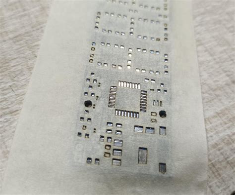
1. Toner Transfer Method
The toner transfer method is a popular and relatively simple approach to DIY PCB fabrication. It involves the following steps:
- Print your PCB layout onto a special toner transfer paper using a laser printer.
- Clean and prepare a copper-clad board.
- Place the toner transfer paper onto the copper-clad board and apply heat and pressure using an iron or laminator.
- Remove the paper, leaving the toner ink on the copper surface.
- Etch away the unwanted copper using a chemical etchant solution, such as ferric chloride or ammonium persulfate.
- Clean the board and drill holes for component placement.
| Pros | Cons |
|---|---|
| Inexpensive | Limited resolution |
| Easily accessible materials | Requires manual alignment |
| Suitable for simple designs | Inconsistent results |
2. Photoresist Method
The photoresist method offers higher precision and resolution compared to the toner transfer method. It involves the following steps:
- Apply a photoresist film or liquid onto a clean copper-clad board.
- Create a transparent film of your PCB layout using a laser printer or inkjet printer with transparency sheets.
- Expose the photoresist-coated board to UV light through the transparent film.
- Develop the photoresist using a developer solution, which removes the unexposed areas.
- Etch away the unwanted copper using a chemical etchant solution.
- Remove the remaining photoresist using a solvent and drill holes for component placement.
| Pros | Cons |
|---|---|
| High resolution and precision | Requires additional equipment (UV exposure unit) |
| Consistent results | More complex process |
| Suitable for complex designs | Higher material cost |
3. CNC Milling
CNC (Computer Numerical Control) milling is a subtractive fabrication method that uses a computer-controlled milling machine to remove copper from a pre-coated board. The process involves the following steps:
- Export your PCB layout as a machine-readable file format, such as Gerber or G-code.
- Set up the CNC milling machine with the appropriate tools and parameters.
- Load the copper-clad board into the machine and secure it.
- Run the milling program, which guides the machine to remove copper based on your PCB layout.
- Clean the board and drill holes for component placement.
| Pros | Cons |
|---|---|
| High precision and accuracy | Requires specialized equipment (CNC machine) |
| Suitable for complex designs | Higher initial investment |
| Rapid prototyping | Limited to subtractive process |

Component Placement and Soldering
After fabricating your PCB, the next step is to place and solder the components onto the board. Here are some tips for successful component placement and soldering:
-
Component Placement: Refer to your schematic and PCB layout to determine the correct placement of each component. Pay attention to the orientation of polarized components like capacitors, diodes, and ICs.
-
Soldering Techniques: Use a soldering iron with an appropriate tip size and temperature for the components you are soldering. Apply heat to both the component lead and the PCB pad simultaneously, and then feed the solder wire to create a strong joint. Avoid overheating the components or applying excessive solder.
-
Inspection and Cleaning: After soldering, visually inspect each joint for any bridges, cold solder joints, or incomplete connections. Use a multimeter to check for continuity and shorts. Clean the board using isopropyl alcohol to remove any flux residue.

Testing and Troubleshooting
Once your PCB is assembled, it’s time to test its functionality and troubleshoot any issues that may arise. Here are some steps to follow:
-
Visual Inspection: Carefully examine the PCB for any visible defects, such as damaged components, incorrect placements, or solder bridges.
-
Power-On Test: Apply power to your PCB and check for any abnormal behavior, such as excessive heat, smoke, or unexpected voltage levels.
-
Functional Testing: Test the individual functions of your PCB by providing the necessary inputs and verifying the expected outputs. Use test points, oscilloscopes, or other diagnostic tools to monitor signals and identify any anomalies.
-
Debugging: If you encounter issues during testing, use a systematic approach to isolate the problem. Check for common issues like incorrect component values, poor solder joints, or software bugs. Consult datasheets, schematics, and online resources for troubleshooting guidance.
Frequently Asked Questions (FAQ)
-
What software can I use to design my PCB?
There are several popular EDA software options available, both free and paid. Some widely used options include KiCad, Eagle, Altium Designer, and Autodesk Fusion 360. These software tools provide schematic capture, PCB layout, and design rule checking capabilities. -
Can I make double-sided or multi-layer PCBs using DIY methods?
Yes, it is possible to create double-sided and multi-layer PCBs using DIY methods. However, the process becomes more complex and requires additional steps, such as precise alignment, double-sided exposure (for photoresist method), and careful drilling of vias to connect layers. -
How do I choose the right components for my PCB?
When selecting components for your PCB, consider factors such as the required electrical specifications (voltage, current, power rating), package size and footprint, availability, and cost. Refer to datasheets and application notes provided by component manufacturers to ensure compatibility and suitability for your design. -
What safety precautions should I take when working with DIY PCBs?
When working with DIY PCBs, prioritize safety. Wear protective gloves and eyewear when handling chemicals like etchants and solvents. Work in a well-ventilated area to avoid inhaling fumes. Use appropriate tools and equipment, such as ESD-safe Soldering Irons and mats, to prevent electrostatic discharge damage to sensitive components. -
Where can I find resources and communities for DIY PCB enthusiasts?
There are numerous online resources and communities dedicated to DIY PCBs and electronics. Websites like instructables.com, hackster.io, and electronics-lab.com offer tutorials, projects, and forums where you can learn from experienced makers and seek guidance. Social media platforms like Reddit (/r/PrintedCircuitBoard) and Facebook groups also provide opportunities to connect with fellow enthusiasts and share knowledge.
Conclusion
Customizing your own circuit boards through DIY PCB fabrication can be a rewarding and educational experience. By understanding the PCB design process, exploring different fabrication methods, and following best practices for component placement and soldering, you can bring your electronic projects to life. Whether you are a hobbyist, student, or professional, the ability to create custom PCBs opens up a world of possibilities for innovation and experimentation.
Remember to prioritize safety, seek guidance when needed, and continuously learn from the vibrant community of DIY PCB enthusiasts. With patience, practice, and perseverance, you can master the art of creating custom circuit boards and take your electronics projects to the next level.
No responses yet