Types of BGA PCB Soldering Defects
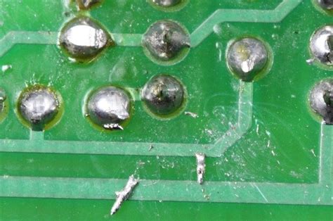
1. Open Joints (Cold Solder Joints)
Open joints, also known as cold solder joints, occur when there is insufficient wetting of the solder to the pad or ball. This results in a weak or non-existent electrical connection.
Causes:
- Insufficient heat during soldering
- Poor fluxing or inadequate flux activity
- Oxidation on the pads or balls
- Incorrect solder paste volume or composition
Prevention:
- Ensure proper reflow profile and temperature control
- Use appropriate flux and maintain proper flux coverage
- Keep components and PCBs clean and free from oxidation
- Optimize solder paste stencil design and printing process
Repair:
- Rework the affected joints using a hot air or infrared rework station
- Add flux and additional solder if necessary
- Clean the area thoroughly after rework
2. Bridging (Short Circuits)
Bridging occurs when solder inadvertently connects two or more adjacent pads or balls, creating a short circuit.
Causes:
- Excessive solder paste volume
- Poor stencil design or misalignment
- Component misplacement
- Inadequate spacing between pads or balls
Prevention:
- Optimize solder paste stencil design and thickness
- Ensure proper stencil alignment and printing process
- Use automated component placement for accurate positioning
- Follow recommended pad and ball spacing guidelines
Repair:
- Remove the excess solder using a solder wick or vacuum desoldering tool
- Use a soldering iron with a fine tip to separate the bridged connections
- Clean the area and inspect for any remaining shorts
3. Head-in-Pillow (HiP) Defects
Head-in-Pillow (HiP) defects occur when the BGA ball and pad make contact but fail to properly collapse and form a strong intermetallic bond.
Causes:
- Oxidation on the ball or pad surface
- Improper reflow profile or insufficient peak temperature
- Poor wetting due to contamination or inadequate fluxing
- Warpage of the component or PCB during reflow
Prevention:
- Maintain proper storage conditions to prevent oxidation
- Optimize the reflow profile and ensure adequate peak temperature
- Use appropriate flux and maintain cleanliness during assembly
- Control the PCB and component warpage through proper design and material selection
Repair:
- Remove the affected component using a rework station
- Clean the pads and replace the component with a new one
- Reflow the new component using the appropriate profile and flux
4. Voiding
Voiding occurs when gas bubbles or pockets form within the solder joint, reducing its strength and electrical conductivity.
Causes:
- Outgassing from the flux or solder paste during reflow
- Trapped moisture or contaminants within the solder joint
- Inappropriate reflow profile or cooling rate
- Uneven solder paste deposition or poor wetting
Prevention:
- Select low-voiding solder paste formulations
- Optimize the reflow profile to minimize outgassing and ensure proper wetting
- Control the cooling rate to allow gases to escape
- Ensure even solder paste deposition through stencil design and printing process
Repair:
- Minor voiding may not require repair if it meets acceptability criteria
- For excessive voiding, remove the affected component and rework the joint
- Use vacuum assist or vapor phase reflow to minimize voiding during rework
BGA PCB Soldering Defect Classification
| Defect Type | Description | Causes | Prevention | Repair |
|---|---|---|---|---|
| Open Joint | Insufficient wetting of solder to pad or ball | – Insufficient heat – Poor fluxing – Oxidation – Incorrect solder paste |
– Proper reflow profile – Appropriate flux – Clean components and PCBs – Optimize solder paste |
– Rework affected joints – Add flux and solder – Clean thoroughly |
| Bridging | Solder connecting adjacent pads or balls | – Excessive solder paste – Poor stencil design – Component misplacement – Inadequate spacing |
– Optimize stencil design – Ensure stencil alignment – Automated component placement – Follow spacing guidelines |
– Remove excess solder – Use fine tip soldering iron – Clean and inspect |
| Head-in-Pillow | Ball and pad contact but fail to collapse | – Oxidation – Improper reflow profile – Poor wetting – Warpage |
– Prevent oxidation – Optimize reflow profile – Use appropriate flux – Control warpage |
– Remove affected component – Clean pads – Replace component – Reflow with proper profile |
| Voiding | Gas bubbles or pockets within solder joint | – Outgassing from flux or paste – Trapped moisture or contaminants – Inappropriate reflow profile – Uneven solder deposition |
– Low-voiding solder paste – Optimize reflow profile – Control cooling rate – Even solder deposition |
– Minor voiding may not require repair – Remove and rework excessive voiding – Use vacuum assist or vapor phase reflow |

BGA PCB Soldering Defect Prevention Guidelines
- Stencil Design and Printing
- Optimize stencil aperture size and shape for each BGA pad
- Ensure proper stencil thickness and alignment
- Maintain consistent solder paste viscosity and printing parameters
-
Regularly clean and inspect the stencil for damage or contamination
-
Reflow Profile Optimization
- Develop a tailored reflow profile for each BGA component and PCB combination
- Ensure adequate preheat, soak, and peak temperature zones
- Control the ramp rates and minimize temperature gradients across the PCB
-
Optimize the cooling rate to allow proper solder joint formation and gas escape
-
Flux Selection and Application
- Choose a flux compatible with the solder paste and BGA component
- Ensure proper flux coverage on the pads and balls
- Avoid excessive flux residue, which can cause contamination or voiding
-
Clean the PCB and components thoroughly after soldering, if required
-
Component Placement Accuracy
- Use automated pick-and-place equipment for precise BGA component placement
- Ensure proper component alignment and coplanarity with the PCB surface
- Verify the placement accuracy using optical inspection or X-ray imaging
-
Implement process controls to prevent component shifting during reflow
-
PCB and Component Warpage Control
- Design the PCB with balanced copper distribution and symmetrical layer stackup
- Choose PCB materials with good thermal stability and low coefficient of thermal expansion (CTE)
- Use appropriate PCB support and clamping during reflow to minimize warpage
-
Select BGA components with matched CTE and rigidity to the PCB
-
Cleanliness and Contamination Control
- Maintain a clean and controlled environment for PCB assembly
- Store PCBs and components in moisture-barrier bags with desiccants
- Bake PCBs and components before assembly to remove excess moisture
- Avoid handling the PCBs and components with bare hands to prevent contamination

Frequently Asked Questions (FAQ)
-
What is the most common BGA soldering defect?
The most common BGA soldering defect is open joints (cold solder joints), which occur due to insufficient wetting of the solder to the pad or ball. This can be caused by factors such as insufficient heat, poor fluxing, oxidation, or incorrect solder paste volume or composition. -
How can I prevent bridging between BGA pads?
To prevent bridging between BGA pads, optimize the solder paste stencil design and thickness, ensure proper stencil alignment and printing process, use automated component placement for accurate positioning, and follow recommended pad and ball spacing guidelines. Proper control of solder paste volume and placement accuracy is crucial to avoiding bridging defects. -
What causes head-in-pillow (HiP) defects in BGA soldering?
Head-in-pillow (HiP) defects in BGA soldering are caused by various factors, including oxidation on the ball or pad surface, improper reflow profile or insufficient peak temperature, poor wetting due to contamination or inadequate fluxing, and warpage of the component or PCB during reflow. These factors prevent the proper collapse and formation of a strong intermetallic bond between the BGA ball and pad. -
How much voiding is acceptable in BGA solder joints?
The acceptability of voiding in BGA solder joints depends on the specific industry standards and customer requirements. Generally, a voiding level of less than 25% of the total joint area is considered acceptable for most applications. However, for critical applications such as aerospace or medical devices, the acceptable voiding level may be more stringent, typically below 10%. -
Can BGA soldering defects be repaired?
Yes, most BGA soldering defects can be repaired using appropriate rework techniques. For open joints, bridging, and excessive voiding, the affected component can be removed using a hot air or infrared rework station, and the pads can be cleaned. A new component can then be placed and reflowed using the appropriate profile and flux. For head-in-pillow defects, the affected component should be removed, the pads cleaned, and a new component placed and reflowed. However, it is important to note that rework can be time-consuming and may affect the overall reliability of the PCB if not performed correctly.

Conclusion
BGA PCB soldering is a complex process that requires careful control of various factors to ensure reliable and defect-free solder joints. By understanding the typical error categories, their causes, prevention, and repair methods, PCB assembly professionals can minimize the occurrence of BGA soldering defects and improve the overall quality of their products.
Implementing best practices such as optimizing stencil design and printing, developing tailored reflow profiles, selecting appropriate flux, ensuring accurate component placement, controlling PCB and component warpage, and maintaining cleanliness and contamination control can greatly reduce the risk of BGA soldering defects.
Regular inspection, testing, and continuous process improvement are essential for identifying and correcting any issues in the BGA soldering process. By staying up-to-date with the latest industry standards, techniques, and equipment, PCB assembly professionals can overcome the challenges associated with BGA soldering and deliver high-quality, reliable electronic products.
No responses yet