Introduction to PCB Soldering
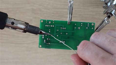
Printed Circuit Board (PCB) soldering is a crucial process in electronics manufacturing that involves joining electronic components to the PCB using molten solder. The quality of the solder joints directly impacts the reliability and performance of the electronic device. One of the most important aspects of PCB soldering is creating a good solder ball, which ensures a strong and stable connection between the component and the PCB.
What is a Solder Ball?
A solder ball is a small sphere of solder that is used to create a connection between an electronic component and a PCB. Solder balls are commonly used in surface mount technology (SMT) assembly, where the components are mounted directly onto the surface of the PCB. The solder balls are placed on the PCB pads, and when heated, they melt and form a strong bond with the component leads.

Why is a Good Solder Ball Important?
A good solder ball is essential for several reasons:
-
Strength: A well-formed solder ball creates a strong mechanical bond between the component and the PCB, ensuring the connection remains intact even under stress or vibration.
-
Conductivity: A properly formed solder ball provides excellent electrical conductivity, allowing signals to pass between the component and the PCB without interference or loss.
-
Reliability: A good solder ball reduces the risk of defects such as cold joints, bridging, or insufficient wetting, which can lead to device failure.
-
Aesthetics: A uniform and well-shaped solder ball gives the PCB a professional appearance and makes it easier to inspect for quality control purposes.

Factors Affecting Solder Ball Quality
Several factors can influence the quality of a solder ball:
Solder Paste
The solder paste is a mixture of powdered solder and flux that is applied to the PCB pads before component placement. The quality and composition of the solder paste can affect the formation of the solder ball. Some key considerations include:
-
Alloy composition: The solder alloy should be chosen based on the specific application requirements, such as melting temperature, strength, and compatibility with the component and PCB materials.
-
Particle size: The size of the solder particles in the paste can impact the flow and wetting characteristics of the molten solder. Smaller particles generally result in better printability and more uniform solder balls.
-
Flux type: The flux in the solder paste helps to remove oxides and improve wetting. The choice of flux depends on the PCB surface finish, component metallization, and cleaning requirements.
Stencil Design
The solder paste is applied to the PCB using a stencil, which is a thin metal sheet with apertures that correspond to the PCB pads. The design of the stencil can significantly affect the volume and shape of the solder paste deposit, and consequently, the solder ball quality. Some important stencil design considerations include:
-
Aperture size: The aperture size should be optimized based on the pad size, pitch, and solder paste properties. Typically, the aperture should be slightly larger than the pad to allow for some paste shrinkage during reflow.
-
Aperture shape: The shape of the aperture can be circular, square, or rectangular, depending on the pad geometry and the desired solder paste volume.
-
Stencil thickness: The thickness of the stencil determines the height of the solder paste deposit. Thicker stencils deposit more paste, resulting in larger solder balls, while thinner stencils produce smaller solder balls.
Reflow Profile
The reflow profile refers to the temperature and time settings used during the soldering process. A well-designed reflow profile ensures that the solder paste melts completely, wets the surfaces properly, and forms a good solder ball. Some key aspects of the reflow profile include:
-
Preheat: The preheat stage gradually raises the PCB temperature to activate the flux and remove volatile solvents from the solder paste.
-
Soak: The soak stage holds the temperature steady to allow the components and PCB to reach thermal equilibrium and promote uniform heating.
-
Reflow: The reflow stage raises the temperature above the melting point of the solder alloy, causing the solder paste to melt and wet the surfaces. The peak temperature and time above liquidus (TAL) should be carefully controlled to ensure complete melting without damaging the components or PCB.
-
Cooling: The cooling stage allows the molten solder to solidify and form the final solder ball shape. The cooling rate should be controlled to minimize thermal shock and prevent defects such as cracking or delamination.
PCB Surface Finish
The surface finish on the PCB pads can affect the wetting and bonding characteristics of the solder ball. Some common PCB surface finishes include:
-
HASL (Hot Air Solder Leveling): A tin-lead alloy is applied to the PCB pads and then leveled using hot air. HASL provides good solderability but can result in uneven pad surfaces.
-
OSP (Organic Solderability Preservative): A thin organic coating is applied to the PCB pads to prevent oxidation and improve solderability. OSP is cost-effective but has a limited shelf life.
-
ENIG (Electroless Nickel Immersion Gold): A layer of nickel is plated onto the PCB pads, followed by a thin layer of gold. ENIG provides excellent solderability and flatness but is more expensive than other finishes.
-
ENEPIG (Electroless Nickel Electroless Palladium Immersion Gold): Similar to ENIG, but with an additional layer of palladium between the nickel and gold layers. ENEPIG offers improved wear resistance and compatibility with various solder alloys.
| Surface Finish | Advantages | Disadvantages |
|---|---|---|
| HASL | – Good solderability – Cost-effective |
– Uneven pad surfaces – Thermal shock |
| OSP | – Cost-effective – Flat pad surfaces |
– Limited shelf life – Sensitive to handling |
| ENIG | – Excellent solderability – Flat pad surfaces |
– Higher cost – Potential for black pad defect |
| ENEPIG | – Excellent solderability – Flat pad surfaces – Improved wear resistance |
– Higher cost – Complex process |
Component Placement
The accuracy and consistency of component placement can impact the solder ball formation. Misaligned or tilted components can lead to uneven solder ball shapes or bridging between adjacent pads. Some key factors in component placement include:
-
Placement accuracy: The placement machine should have high accuracy and repeatability to ensure precise positioning of the components on the PCB pads.
-
Placement force: The force applied during component placement should be sufficient to maintain the component position without damaging the component or PCB.
-
Placement speed: The placement speed should be optimized to achieve high throughput without compromising placement accuracy or causing component skidding.

Best Practices for Creating Good Solder Balls
To create good solder balls consistently, consider the following best practices:
-
Select the appropriate solder paste: Choose a solder paste with the right alloy composition, particle size, and flux type for your specific application.
-
Optimize stencil design: Design the stencil apertures to achieve the desired solder paste volume and shape on the PCB pads.
-
Control the reflow profile: Develop a reflow profile that ensures complete solder melting, proper wetting, and minimal thermal stress on the components and PCB.
-
Choose a suitable PCB surface finish: Select a PCB surface finish that provides good solderability, flatness, and compatibility with the solder alloy.
-
Ensure accurate component placement: Use a high-quality placement machine and optimize the placement parameters to achieve precise and consistent component positioning.
-
Implement quality control measures: Regularly inspect the solder balls for quality using visual inspection, X-ray analysis, or cross-sectioning. Monitor process parameters and maintain equipment to ensure consistent results.
Troubleshooting Common Solder Ball Issues
Despite best efforts, solder ball issues can still occur. Here are some common problems and their potential solutions:
Insufficient Solder Volume
If the solder balls are too small or flat, it may be due to insufficient solder paste volume. Possible solutions include:
- Increasing the stencil aperture size or thickness
- Checking the solder paste for proper viscosity and consistency
- Verifying the stencil alignment and cleanliness
Excessive Solder Volume
If the solder balls are too large or bulging, it may be due to excessive solder paste volume. Possible solutions include:
- Reducing the stencil aperture size or thickness
- Adjusting the solder paste print parameters (speed, pressure, separation)
- Checking for stencil damage or contamination
Bridging
Bridging occurs when solder balls from adjacent pads merge together, creating an unintended connection. Possible solutions include:
- Reducing the solder paste volume
- Increasing the pad spacing or solder mask opening
- Adjusting the reflow profile to improve solder wetting and separation
- Verifying component placement accuracy
Head-in-Pillow (HIP)
HIP defects occur when the solder ball on the component does not fully collapse and merge with the solder paste on the PCB pad. Possible solutions include:
- Ensuring proper flux activation and wetting during reflow
- Verifying component and PCB pad cleanliness and surface finish compatibility
- Adjusting the reflow profile to achieve adequate peak temperature and time above liquidus
- Checking for component warpage or damage
FAQ
1. What is the most common solder alloy used for PCB soldering?
The most common solder alloy for PCB soldering is SAC305, which contains 96.5% tin (Sn), 3% silver (Ag), and 0.5% copper (Cu). This lead-free alloy has a melting point of around 217°C and provides good strength, reliability, and wetting properties.
2. How do I choose the right solder paste for my application?
When selecting a solder paste, consider factors such as the solder alloy composition, particle size, flux type, and viscosity. The alloy should be compatible with the component and PCB metallization, while the particle size and viscosity should suit the stencil design and printing process. The flux type should provide adequate activity and cleaning characteristics for the specific PCB surface finish and assembly environment.
3. What is the optimal reflow profile for achieving good solder balls?
The optimal reflow profile depends on the specific solder paste and PCB assembly characteristics. However, a typical lead-free reflow profile includes a preheat stage (ramp rate: 1-3°C/s, temperature: 150-180°C), a soak stage (60-120 seconds at 150-180°C), a reflow stage (peak temperature: 235-250°C, time above liquidus: 60-90 seconds), and a cooling stage (ramp rate: 3-6°C/s). The exact parameters should be fine-tuned based on the solder paste manufacturer’s recommendations and empirical testing.
4. How can I prevent solder ball bridging?
To prevent solder ball bridging, consider the following measures:
- Optimize the solder paste volume and stencil design to avoid excessive paste deposition
- Ensure adequate pad spacing and solder mask opening to prevent solder paste spreading
- Verify component placement accuracy to maintain proper alignment and spacing
- Adjust the reflow profile to promote proper solder wetting and separation
5. What are some methods for inspecting solder ball quality?
Solder ball quality can be inspected using various methods, including:
- Visual inspection: Use a magnifying lens or microscope to examine solder ball shape, size, and wetting
- X-ray analysis: Use 2D or 3D X-ray imaging to assess solder ball position, volume, and internal structure
- Cross-sectioning: Cut the PCB and component to examine the solder ball cross-section and intermetallic formation
- Automated optical inspection (AOI): Use machine vision systems to detect solder ball defects and measure dimensions
By implementing best practices, troubleshooting common issues, and regularly inspecting solder ball quality, you can ensure reliable and high-performance PCB assemblies.
Conclusion
Creating a good solder ball is essential for achieving strong, reliable, and high-quality PCB assemblies. By understanding the factors that influence solder ball formation, such as solder paste selection, stencil design, reflow profile, PCB surface finish, and component placement, you can optimize your process to consistently produce well-formed solder balls.
Implementing best practices, troubleshooting common issues, and regularly monitoring solder ball quality through visual inspection, X-ray analysis, cross-sectioning, and automated optical inspection can help you maintain high standards and minimize defects.
As PCB technology continues to advance, with smaller components, finer pitch, and more complex designs, the importance of good solder ball formation will only increase. By staying informed about the latest materials, processes, and quality control methods, you can ensure that your PCB assemblies meet the ever-growing demands of the electronics industry.
No responses yet