What is PCB Testing?
PCB testing is the process of verifying that a printed circuit board (PCB) functions as intended and meets all required specifications. This involves a series of tests and inspections at various stages of the PCB manufacturing process, from the initial prototype to the final assembled board.
The main goals of PCB testing are to:
– Ensure the PCB design is correct and free of errors
– Verify the PCB fabrication process was carried out correctly
– Confirm all components are properly soldered and connected
– Detect any defects or issues that could affect the PCB’s performance or reliability
By thoroughly testing PCBs, manufacturers can identify and resolve problems early on, reducing the risk of costly failures or recalls later in the product lifecycle.
Types of PCB Testing
There are several types of PCB tests that can be performed, depending on the stage of production and the specific requirements of the project. Some of the most common types of PCB testing include:
1. Design Rule Checking (DRC)
Design Rule Checking is a software-based test that verifies the PCB design complies with a set of predefined rules and constraints. These rules are based on the manufacturing capabilities of the PCB fabricator and the requirements of the end application.
DRC checks for issues such as:
– Minimum trace widths and spacing
– Hole sizes and pad dimensions
– Copper pour and clearance
– Silk screen and solder mask clearance
By running DRC on the PCB design files, designers can catch and fix errors before the board is sent for fabrication, saving time and money.
2. Bare Board Testing
Bare board testing is performed on the PCB substrate after fabrication, but before any components are attached. The purpose of bare board testing is to verify the PCB was manufactured correctly and meets all the specified electrical and physical properties.
Some common bare board tests include:
| Test | Description |
|---|---|
| Visual Inspection | A manual or automated optical inspection of the PCB surface for defects such as scratches, dents, or discoloration |
| Continuity Test | Checks for short circuits or open circuits between the PCB’s conductive paths |
| Insulation Resistance Test | Measures the resistance between isolated conductors to ensure adequate insulation |
| Dielectric Withstanding Voltage Test | Applies a high voltage between conductors to check for insulation breakdown or leakage current |
3. In-Circuit Testing (ICT)
In-circuit testing is performed after the PCB has been populated with components, but before the final assembly is completed. ICT uses a bed-of-nails fixture to make electrical contact with specific points on the PCB and verifies the presence, orientation, and value of each component.
ICT can detect issues such as:
– Missing or incorrectly placed components
– Backwards or upside-down components
– Incorrect component values (e.g. wrong resistor or capacitor values)
– Short circuits or open circuits caused by soldering defects
ICT is an automated test that can quickly identify assembly defects and ensure the PCB is ready for final assembly and functional testing.
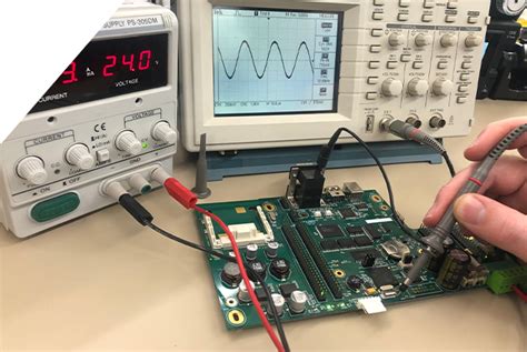
4. Functional Testing
Functional testing is performed on the fully assembled PCB to verify it operates as intended and meets all the specified performance requirements. Functional tests are designed to simulate the real-world operating conditions of the PCB and check for proper functionality, timing, and signal integrity.
Functional tests can be performed at various levels, such as:
| Test Level | Description |
|---|---|
| Component Level | Verifies each individual component on the PCB is functioning correctly |
| Circuit Block Level | Checks the operation of specific circuits or functional blocks on the PCB |
| System Level | Tests the complete PCB Assembly as a whole, including any external interfaces or peripherals |
Functional testing often involves the use of specialized test equipment, such as oscilloscopes, logic analyzers, and signal generators, to stimulate the PCB inputs and measure the outputs.
5. Burn-In Testing
Burn-in testing is a type of accelerated life testing that subjects the PCB to elevated temperatures and voltages for an extended period of time. The purpose of burn-in testing is to identify any early-life failures or defects that may not be detected by other tests.
During burn-in testing, the PCB is typically placed in a temperature-controlled chamber and powered on for a specified duration, usually several hours or days. The elevated temperature and voltage stress can cause weak components or marginal solder joints to fail prematurely, allowing them to be identified and replaced before the PCB is shipped to the customer.
Burn-in testing is often used for high-reliability applications, such as aerospace, military, or medical devices, where the cost of failure is high and long-term reliability is critical.

PCB Testing Equipment
To perform the various types of PCB tests, manufacturers use a range of specialized equipment and tools. Some of the most common PCB testing equipment includes:
1. Automatic Optical Inspection (AOI) Machines
AOI machines are used to visually inspect the PCB surface for defects such as missing components, solder bridging, or poor solder joints. AOI systems use high-resolution cameras and advanced image processing algorithms to quickly scan the PCB and compare it to a reference image.
2. Flying Probe Testers
Flying probe testers are used for bare board testing and in-circuit testing. They use a set of movable probes to make electrical contact with specific points on the PCB and perform continuity, resistance, and voltage tests. Flying probe testers are flexible and can be programmed to test a wide variety of PCB designs.
3. Bed-of-Nails Fixtures
Bed-of-nails fixtures are used for in-circuit testing of populated PCBs. They consist of a custom-designed plate with a grid of spring-loaded pins that make contact with the PCB test points. The fixture is connected to a test system that applies electrical signals and measures the response of the PCB.
4. Functional Test Systems
Functional test systems are used to verify the complete functionality of the assembled PCB. They can include a variety of instruments, such as power supplies, signal generators, oscilloscopes, and data acquisition modules, as well as custom software to automate the test sequence and analyze the results.
5. Environmental Test Chambers
Environmental test chambers are used for burn-in testing and other environmental stress tests. They can control the temperature, humidity, and pressure inside the chamber to simulate various operating conditions and identify any weaknesses or failures in the PCB.

PCB Testing Process
The PCB testing process typically involves several stages, from the initial design review to the final functional testing. Here is an overview of the main steps in the PCB testing process:
-
Design Review: The PCB design files are reviewed for completeness, accuracy, and compliance with manufacturing and assembly standards. Any issues or discrepancies are identified and corrected before proceeding to fabrication.
-
DRC: The PCB design undergoes a DRC to ensure it meets all the specified design rules and constraints. Any violations or errors are flagged and corrected by the designer.
-
Bare Board Testing: After fabrication, the bare PCB is tested for continuity, insulation resistance, and dielectric strength. Any defects or issues are identified and the board is either reworked or scrapped.
-
Assembly Inspection: After the PCB is populated with components, it undergoes a visual inspection to check for proper component placement, orientation, and solder joint quality. Any defects are corrected before proceeding to in-circuit testing.
-
In-Circuit Testing: The populated PCB is tested using a bed-of-nails fixture or flying probe tester to verify the presence, orientation, and value of each component. Any missing or incorrect components are identified and replaced.
-
Functional Testing: The fully assembled PCB is tested for functionality, performance, and compatibility with other system components. Any issues are debugged and corrected before the PCB is approved for final assembly.
-
Burn-In Testing: For high-reliability applications, the PCB may undergo a burn-in test to identify any early-life failures or weaknesses. Any defective boards are reworked or scrapped.
-
Final Inspection: Before shipping, the PCB undergoes a final visual inspection and functional test to ensure it meets all the required specifications and quality standards.
By following this multi-stage testing process, PCB manufacturers can ensure the quality and reliability of their products and minimize the risk of defects or failures in the field.

PCB Testing Challenges and Best Practices
While PCB testing is a critical step in the manufacturing process, it can also present some challenges and potential pitfalls. Here are some common PCB testing challenges and best practices for overcoming them:
Challenges
-
Complexity: As PCBs become more complex and dense, with higher layer counts and smaller feature sizes, testing becomes more difficult and time-consuming. This can lead to increased costs and longer production cycles.
-
Accessibility: Some PCB designs may have limited access points for testing, making it difficult to probe or inspect certain areas of the board. This can require specialized fixtures or techniques to ensure adequate test coverage.
-
Variability: PCBs can be subject to variability in materials, processes, and environmental conditions, which can affect their performance and reliability. This can make it challenging to establish consistent test criteria and thresholds.
-
Cost: PCB testing equipment and labor can be expensive, especially for high-volume production runs. Balancing test coverage and cost is a constant challenge for manufacturers.
Best Practices
-
Design for Testability: PCB designers should consider testability early in the design process, incorporating features such as test points, access vias, and clear labeling to facilitate testing and inspection.
-
Establish Clear Specifications: Manufacturers should work closely with their customers to establish clear and comprehensive specifications for the PCB, including all functional, environmental, and quality requirements.
-
Use Automated Testing: Automated test equipment, such as AOI and flying probe testers, can help reduce testing time and improve consistency and accuracy compared to manual methods.
-
Implement Statistical Process Control: By monitoring key process parameters and test results over time, manufacturers can identify trends and variations that may indicate potential issues or opportunities for improvement.
-
Collaborate with Suppliers: Manufacturers should work closely with their PCB fabrication and component suppliers to ensure consistent quality and reliability throughout the supply chain.
By following these best practices and continually improving their testing processes and capabilities, PCB manufacturers can deliver high-quality, reliable products to their customers while minimizing costs and time to market.
FAQ
1. What is the difference between PCB testing and inspection?
PCB testing involves applying electrical signals to the board and measuring its response to verify functionality, while inspection involves visually examining the board for defects or anomalies without applying power.
2. How much does PCB testing cost?
The cost of PCB testing can vary widely depending on the complexity of the board, the volume of production, and the type of tests required. In general, testing can account for 5-20% of the total PCB Manufacturing Cost.
3. Can all PCB defects be detected by testing?
While PCB testing can catch most common defects, such as opens, shorts, and incorrect component values, some issues may be difficult or impossible to detect through standard test methods. These can include intermittent faults, timing-related issues, or defects that only manifest under specific operating conditions.
4. How long does PCB testing take?
The duration of PCB testing can range from a few minutes to several hours, depending on the complexity of the board and the type of tests being performed. In general, bare board testing and in-circuit testing are faster than functional testing and burn-in testing.
5. What is the role of PCB testing in product quality and reliability?
PCB testing plays a critical role in ensuring the quality and reliability of electronic products. By identifying and correcting defects early in the manufacturing process, testing can help prevent costly failures and recalls later on, while also improving customer satisfaction and brand reputation. Effective PCB testing requires a combination of advanced equipment, skilled personnel, and robust processes and standards.
No responses yet