Introduction to Copper Clad Laminate
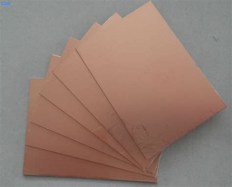
Copper Clad Laminate (CCL) is a crucial component in the manufacturing of printed circuit boards (PCBs). It consists of a thin layer of copper foil bonded to a dielectric substrate, typically made of glass-reinforced epoxy resin or other insulating materials. CCL serves as the foundation for creating conductive patterns on PCBs, which are essential for electronic devices’ functionality.
Composition of Copper Clad Laminate
Copper Clad Laminate is composed of three main components:
- Copper foil
- Dielectric substrate
- Bonding agent
The copper foil is a thin sheet of pure copper, usually ranging from 1/8 oz to 10 oz in thickness. The dielectric substrate is an insulating material that provides mechanical support and electrical insulation. The most common substrates used in CCL are:
- FR-4 (Flame Retardant 4): A glass-reinforced epoxy laminate
- CEM-1 (Composite Epoxy Material 1): A paper-based phenolic resin laminate
- CEM-3: A glass-reinforced epoxy laminate with a non-woven glass reinforcement
The bonding agent, typically an epoxy resin, is used to adhere the copper foil to the dielectric substrate.
Manufacturing Process of Copper Clad Laminate
The manufacturing process of CCL involves several steps:
-
Substrate Preparation: The dielectric substrate is cut to the desired size and shape. It is then cleaned and treated to improve adhesion.
-
Copper Foil Preparation: The copper foil is also cut to the appropriate size and cleaned to remove any contaminants.
-
Lamination: The prepared substrate and copper foil are placed in a lamination press. Heat and pressure are applied to bond the copper foil to the substrate using the bonding agent.
-
Cooling: After lamination, the CCL is cooled to room temperature.
-
Inspection: The CCL is inspected for any defects, such as delamination, blistering, or impurities.
Lamination Process Parameters
The lamination process is critical in ensuring the quality and reliability of CCL. The key parameters that influence the lamination process are:
| Parameter | Description | Typical Range |
|---|---|---|
| Temperature | The temperature at which the lamination press operates | 180°C – 200°C |
| Pressure | The pressure applied by the lamination press | 200 – 400 psi |
| Time | The duration of the lamination process | 60 – 120 minutes |
These parameters may vary depending on the specific type of CCL and the manufacturer’s recommendations.

Types of Copper Clad Laminate
There are several types of CCL available, each with unique characteristics and applications.
FR-4 Copper Clad Laminate
FR-4 is the most widely used CCL in the PCB industry. It offers excellent mechanical and electrical properties, making it suitable for a wide range of applications. Key features of FR-4 CCL include:
- High glass transition temperature (Tg): 130°C – 140°C
- Good insulation resistance
- Low dielectric constant and loss tangent
- Excellent dimensional stability
CEM-1 Copper Clad Laminate
CEM-1 is a paper-based phenolic resin laminate that is less expensive than FR-4. It is suitable for low-end, consumer-grade electronics. However, it has lower mechanical and thermal properties compared to FR-4.
CEM-3 Copper Clad Laminate
CEM-3 is a glass-reinforced epoxy laminate with a non-woven glass reinforcement. It offers better mechanical and thermal properties than CEM-1 but is still less expensive than FR-4. CEM-3 is often used in automotive and industrial applications.
High-Frequency Copper Clad Laminate
High-frequency CCL is designed for applications that require low dielectric loss and stable dielectric constant at high frequencies. These laminates are used in high-speed digital and RF/microwave applications. Examples of high-frequency CCL include:
- PTFE (Polytetrafluoroethylene) based laminates
- Hydrocarbon ceramic laminates
- Low-loss glass-reinforced laminates

Applications of Copper Clad Laminate
Copper Clad Laminate is used in a wide range of electronic applications, including:
- Consumer electronics: Smartphones, laptops, tablets, wearables, etc.
- Automotive electronics: Engine control units, infotainment systems, sensors, etc.
- Industrial electronics: Power supplies, motor controls, automation systems, etc.
- Medical devices: Diagnostic equipment, monitoring systems, implantable devices, etc.
- Aerospace and defense: Avionics, radar systems, satellite communication, etc.
The choice of CCL for a specific application depends on various factors, such as the operating environment, electrical requirements, mechanical stresses, and cost constraints.

Advantages of Copper Clad Laminate
Copper Clad Laminate offers several advantages in PCB manufacturing:
- Excellent electrical conductivity: The copper foil provides a low-resistance path for electrical signals.
- Good thermal conductivity: CCL helps dissipate heat generated by electronic components.
- Mechanical stability: The dielectric substrate provides mechanical support and protects the copper circuitry.
- Versatility: CCL is available in various grades and specifications, making it suitable for a wide range of applications.
- Cost-effectiveness: CCL is a relatively inexpensive material compared to other PCB Substrates.
Challenges and Future Trends in Copper Clad Laminate
As electronic devices become more advanced and compact, there is a growing demand for high-performance CCL. Some of the challenges and future trends in CCL development include:
- Miniaturization: Thinner and more compact CCL is required to accommodate smaller and denser PCB Designs.
- High-speed applications: CCL with lower dielectric loss and stable dielectric constant is needed for high-speed digital and RF applications.
- Thermal management: Improved thermal conductivity is essential for managing heat dissipation in high-power applications.
- Environmental concerns: There is a growing demand for eco-friendly and halogen-free CCL materials.
- Cost reduction: Manufacturers are constantly seeking ways to reduce the cost of CCL without compromising performance.
Researchers and manufacturers are working on developing new materials and processes to address these challenges and meet the evolving needs of the electronics industry.
Frequently Asked Questions (FAQ)
-
What is the difference between copper foil thickness and copper weight?
Copper foil thickness is the actual thickness of the copper layer, measured in microns or mils. Copper weight, on the other hand, is the mass of copper per unit area, typically expressed in ounces per square foot (oz/ft²). A common conversion is: 1 oz/ft² = 35 microns (1.4 mils) of copper thickness. -
Can Copper Clad Laminate be recycled?
Yes, CCL can be recycled. The copper foil can be separated from the dielectric substrate and recycled as scrap metal. The substrate, depending on its composition, can also be recycled or repurposed. However, the recycling process for CCL is complex and not widely available. -
What is the shelf life of Copper Clad Laminate?
The shelf life of CCL depends on the storage conditions and the specific type of laminate. In general, CCL should be stored in a cool, dry place, away from direct sunlight and sources of heat. When stored properly, most CCL has a shelf life of 6 to 12 months. -
How do I select the right Copper Clad Laminate for my application?
Selecting the right CCL involves considering several factors, such as the operating environment, electrical requirements, mechanical stresses, and cost constraints. Consult with CCL manufacturers or PCB design experts to determine the most suitable laminate for your specific application. -
What is the role of the bonding agent in Copper Clad Laminate?
The bonding agent, typically an epoxy resin, serves to adhere the copper foil to the dielectric substrate. It ensures a strong and reliable bond between the two components, preventing delamination and maintaining the structural integrity of the CCL.
Conclusion
Copper Clad Laminate is a fundamental material in the production of printed circuit boards. Its unique combination of electrical conductivity, mechanical stability, and versatility makes it an essential component in a wide range of electronic applications. As the electronics industry continues to evolve, there is a growing demand for high-performance, eco-friendly, and cost-effective CCL solutions.
By understanding the composition, manufacturing process, types, and applications of CCL, engineers and designers can make informed decisions when selecting the most suitable laminate for their projects. As researchers and manufacturers work towards addressing the challenges and future trends in CCL development, we can expect to see innovative solutions that will drive the advancement of electronic devices in the years to come.
No responses yet