Introduction to PCB Assembly
Printed Circuit Board (PCB) assembly is the process of creating electronic circuits by mounting components onto a PCB. It involves several steps, including PCB design, component selection, solder paste application, component placement, soldering, and inspection. PCB assembly is a crucial aspect of electronics manufacturing, as it determines the functionality, reliability, and quality of the final product.
Types of PCB Assembly
There are three main types of PCB assembly:
- Through-Hole Assembly (THA)
- Surface Mount Assembly (SMT)
- Mixed Assembly
Through-Hole Assembly (THA)
THA is the traditional method of PCB assembly, where component leads are inserted into drilled holes on the PCB and soldered onto the opposite side. This method is suitable for larger components and provides strong mechanical connections. However, it is slower and less efficient compared to SMT.
Surface Mount Assembly (SMT)
SMT is a more modern approach to PCB assembly, where components are mounted directly onto the surface of the PCB. This method allows for smaller components, higher component density, and faster assembly speeds. SMT has largely replaced THA in most applications due to its numerous advantages.
Mixed Assembly
Mixed assembly combines both THA and SMT techniques on a single PCB. This approach is used when certain components are not available in SMT packages or when specific mechanical requirements need to be met.
PCB Assembly Process
The PCB assembly process involves several key steps:
1. PCB Design
The first step in PCB assembly is designing the circuit board. This involves creating a schematic diagram, selecting components, and designing the PCB layout. The PCB design must consider factors such as signal integrity, power distribution, thermal management, and manufacturability.
2. PCB Fabrication
Once the PCB design is finalized, the bare PCBs are fabricated. This process involves printing the circuit pattern onto a copper-clad substrate, etching away the unwanted copper, drilling holes, and applying a protective solder mask and silkscreen.
3. Solder Paste Application
In SMT Assembly, solder paste is applied to the PCB pads using a stencil or screen printing process. The solder paste consists of tiny solder particles suspended in a flux matrix, which helps to clean and protect the metal surfaces during soldering.
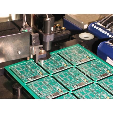
4. Component Placement
The next step is to place the components onto the PCB. In SMT assembly, this is done using automated pick-and-place machines, which can rapidly and accurately place hundreds of components per minute. In THA, components are inserted manually or with the help of semi-automated machines.
5. Soldering
After component placement, the PCB is heated in a reflow oven to melt the solder paste and create a permanent electrical and mechanical connection between the components and the PCB. In THA, soldering is typically done using a wave soldering machine or by hand.
6. Inspection and Testing
The assembled PCBs undergo various inspection and testing procedures to ensure quality and functionality. This may include visual inspection, automated optical inspection (AOI), X-ray inspection, in-circuit testing (ICT), and functional testing.

Benefits of Professional PCB Assembly Services
Outsourcing PCB assembly to professional service providers offers several benefits:
-
Cost Savings: Professional PCB assembly companies have the expertise, equipment, and economies of scale to offer competitive pricing and help reduce overall production costs.
-
Quality Assurance: Experienced PCB assembly providers have stringent quality control processes and use state-of-the-art equipment to ensure consistent, high-quality results.
-
Faster Turnaround Times: With automated processes and streamlined workflows, professional assembly services can deliver PCBs faster than in-house assembly, reducing time-to-market.
-
Access to Expertise: PCB assembly companies have teams of skilled engineers and technicians who can provide valuable insights and support throughout the manufacturing process.
-
Scalability: Outsourcing PCB assembly allows companies to easily scale their production up or down based on demand, without investing in additional equipment or personnel.

Choosing the Right PCB Assembly Partner
When selecting a PCB assembly partner, consider the following factors:
-
Experience and Expertise: Look for a company with a proven track record in PCB assembly and experience in your specific industry or application.
-
Quality Standards: Ensure that the provider adheres to recognized quality standards, such as ISO 9001, IPC-A-610, and J-STD-001.
-
Technology and Equipment: Choose a partner that invests in advanced assembly equipment and keeps up with the latest industry trends and technologies.
-
Communication and Support: Effective communication and responsive support are essential for a successful partnership. Look for a provider that values open communication and offers reliable customer support.
-
Pricing and Lead Times: Compare pricing and lead times from multiple providers to find the best value for your needs. However, be cautious of extremely low prices, as they may indicate compromises in quality or service.

PCB Assembly Challenges and Solutions
PCB assembly comes with its own set of challenges, but there are solutions to overcome them:
Challenge 1: Miniaturization
As electronic devices become smaller and more complex, PCB assembly must adapt to handle tiny components and high-density designs.
Solution: Invest in advanced assembly equipment, such as high-precision pick-and-place machines and microscopes, and train personnel in handling miniaturized components.
Challenge 2: Thermal Management
High-power components and dense PCB layouts can generate significant heat, which can impact performance and reliability.
Solution: Incorporate thermal management techniques into the PCB design, such as using thermal vias, heatsinks, and proper component placement. Use thermally conductive materials and consider thermal simulation during the design phase.
Challenge 3: Electrostatic Discharge (ESD)
ESD can damage sensitive electronic components during the assembly process.
Solution: Implement ESD Protection measures, such as using ESD-safe workstations, grounding equipment, and training personnel in ESD best practices.
Challenge 4: Rework and Repair
Despite best efforts, some assembled PCBs may require rework or repair due to component failures or assembly errors.
Solution: Develop a well-defined rework and repair process, invest in specialized tools and equipment, and train personnel in rework techniques. Regularly analyze rework data to identify and address root causes of defects.
Future Trends in PCB Assembly
The PCB assembly industry is constantly evolving, driven by advances in technology and changing market demands. Some key trends shaping the future of PCB assembly include:
-
Increased Automation: Continued development of automated assembly equipment, such as smart factories and autonomous robotics, will further streamline the assembly process and improve efficiency.
-
Advanced Materials: The adoption of advanced PCB materials, such as high-frequency laminates, flexible substrates, and embedded components, will enable new design possibilities and enhance performance.
-
3D Printing: The integration of 3D printing technology in PCB assembly will allow for the creation of complex, three-dimensional circuit structures and enable rapid prototyping.
-
Internet of Things (IoT): The growing demand for IoT devices will drive the need for low-cost, high-volume PCB assembly solutions optimized for connectivity and low power consumption.
-
Environmental Sustainability: There will be an increased focus on environmentally friendly PCB assembly practices, such as the use of lead-free solders, recyclable materials, and energy-efficient processes.
Conclusion
PCB assembly is a vital process in the production of electronic devices, and its importance will only continue to grow as technology advances. By understanding the various aspects of PCB assembly, from the different types and processes to the benefits of professional services and future trends, companies can make informed decisions when it comes to their PCB assembly needs. Partnering with the right PCB assembly provider and staying up-to-date with industry developments will be crucial for success in this dynamic field.
Frequently Asked Questions (FAQ)
1. What is the difference between THA and SMT PCB assembly?
THA (Through-Hole Assembly) involves inserting component leads through drilled holes in the PCB and soldering them on the opposite side. SMT (Surface Mount Assembly) mounts components directly onto the surface of the PCB. SMT allows for smaller components, higher density, and faster assembly compared to THA.
2. How do I choose the right PCB assembly partner?
When selecting a PCB assembly partner, consider factors such as their experience and expertise in your industry, quality standards, technology and equipment, communication and support, pricing, and lead times. Look for a provider that offers the best combination of these factors to meet your specific needs.
3. What are some common challenges in PCB assembly, and how can they be addressed?
Common challenges in PCB assembly include miniaturization, thermal management, electrostatic discharge (ESD), and rework and repair. These challenges can be addressed by investing in advanced equipment and materials, incorporating appropriate design techniques, implementing ESD protection measures, and developing well-defined rework and repair processes.
4. What are some future trends in PCB assembly?
Future trends in PCB assembly include increased automation, the use of advanced materials, the integration of 3D printing technology, the growth of IoT devices, and a focus on environmental sustainability. Staying informed about these trends can help companies adapt and remain competitive in the evolving PCB assembly landscape.
5. Why should I outsource PCB assembly to a professional service provider?
Outsourcing PCB assembly to a professional service provider offers several benefits, including cost savings, quality assurance, faster turnaround times, access to expertise, and scalability. By leveraging the resources and experience of a dedicated assembly partner, companies can focus on their core competencies while ensuring high-quality, reliable PCB assembly.
| Type of PCB Assembly | Characteristics | Advantages | Disadvantages |
|---|---|---|---|
| Through-Hole Assembly (THA) | Components inserted into drilled holes and soldered on the opposite side | Strong mechanical connections, suitable for large components | Slower assembly, lower component density |
| Surface Mount Assembly (SMT) | Components mounted directly onto the PCB surface | Smaller components, higher density, faster assembly | Requires specialized equipment and processes |
| Mixed Assembly | Combines THA and SMT on a single PCB | Accommodates components not available in SMT, meets specific mechanical requirements | More complex assembly process |
| PCB Assembly Step | Description |
|---|---|
| PCB Design | Creating a schematic diagram, selecting components, and designing the PCB layout |
| PCB Fabrication | Printing the circuit pattern, etching copper, drilling holes, and applying solder mask and silkscreen |
| Solder Paste Application | Applying solder paste to PCB pads using a stencil or screen printing process |
| Component Placement | Placing components onto the PCB, using automated pick-and-place machines for SMT or manual/semi-automated methods for THA |
| Soldering | Melting solder paste in a reflow oven (SMT) or using wave soldering or hand soldering (THA) |
| Inspection and Testing | Conducting visual inspection, AOI, X-ray inspection, ICT, and functional testing to ensure quality and functionality |
No responses yet