What is a PCB Board Blank?
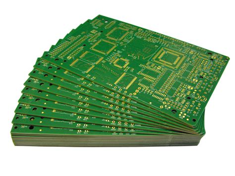
A PCB (printed circuit board) board blank is the starting material used to manufacture PCBs. It consists of a flat sheet of insulating material, typically fiberglass, coated with a thin layer of conductive copper foil on one or both sides. This raw board provides the foundation onto which electronic components and wiring are added to create a functional printed circuit board.
PCB board blanks come in various standard sizes, thicknesses, and materials to suit different applications. The most common types are:
| Type | Description |
|---|---|
| Single-sided | Copper layer on one side of the insulating substrate |
| Double-sided | Copper layers on both sides of the insulating substrate |
| Multi-layer | Multiple copper layers separated by insulating layers |
The choice of PCB board blank depends on the complexity of the circuit design, the required electrical properties, and the intended operating environment.
Factors to Consider When Choosing a PCB Board Blank
Size and Thickness
PCB board blanks are available in standard sizes, such as:
- 100mm x 100mm
- 150mm x 200mm
- 200mm x 300mm
- 300mm x 400mm
The size is chosen based on the dimensions of the circuit design and the space constraints of the device housing. It’s important to select a size that accommodates all the necessary components while leaving room for mounting holes and edge clearance.
The thickness of the PCB board blank is measured in terms of the insulating substrate and the copper foil. Standard thicknesses range from 0.4mm to 3.2mm, with 1.6mm being the most common. Thicker boards provide better mechanical strength and heat dissipation, but are more difficult to route and drill.
Material
The most widely used insulating substrate material for PCB board blanks is FR-4, a flame-retardant fiberglass-reinforced epoxy laminate. FR-4 offers good mechanical and electrical properties, as well as excellent heat resistance. Other materials include:
- Polyimide: High-temperature resistance, used in aerospace and military applications
- Teflon: Low dielectric constant, suitable for high-frequency RF circuits
- Aluminum: Metal-core PCBs for LED lighting and power electronics
The choice of copper foil thickness depends on the current-carrying requirements of the circuit. Thinner foils (e.g., 1 oz/ft²) are used for low-power signal traces, while thicker foils (e.g., 2-4 oz/ft²) are used for high-current power traces.
Copper Weight
The amount of copper on a PCB board blank is specified in terms of weight per unit area, typically ounces per square foot (oz/ft²). Common copper weights are:
| Copper Weight (oz/ft²) | Thickness (μm) |
|---|---|
| 0.5 | 17.5 |
| 1 | 35 |
| 2 | 70 |
| 3 | 105 |
Higher copper weights provide lower resistance and better heat dissipation, but are more expensive and harder to etch fine features.
Surface Finish
The exposed copper on a PCB board blank will oxidize quickly if left unprotected. To prevent oxidation and improve solderability, various surface finishes can be applied:
-
HASL (Hot Air Solder Leveling): A tin-lead alloy is coated onto the copper and leveled by hot air. Provides good solderability but limited flatness.
-
ENIG (Electroless Nickel Immersion Gold): A thin layer of gold is deposited over a nickel barrier layer. Offers excellent flatness and corrosion resistance.
-
OSP (Organic Solderability Preservative): A thin organic coating is applied to protect the copper. Provides good solderability but limited shelf life.
-
Immersion Silver: A thin layer of silver is chemically deposited onto the copper. Offers good solderability and low cost.
The choice of surface finish depends on the assembly process, the expected operating environment, and the shelf life requirements.

PCB Board Blank Manufacturing Process
The manufacturing process for PCB board blanks involves several steps:
-
Lamination: The insulating substrate (e.g., FR-4) is sandwiched between layers of copper foil and bonded together under high pressure and temperature. The number of layers determines whether the board is single-sided, double-sided, or multi-layer.
-
Drilling: Holes are drilled through the board to accommodate through-hole components and vias. The holes are typically drilled using CNC machines with carbide drill bits.
-
Plating: The drilled holes are plated with copper to provide electrical connectivity between layers. This is done by electroless copper deposition followed by electrolytic copper plating.
-
Etching: The unwanted copper is removed from the board using a photolithographic process. A photoresist layer is applied, exposed through a patterned mask, and developed. The exposed copper is then etched away using a chemical solution, leaving only the desired circuit traces.
-
Solder Mask: A layer of insulating material is applied over the copper traces, leaving only the pads and holes exposed. This protects the circuitry from damage and prevents solder bridges during assembly.
-
Silkscreen: A layer of ink is printed onto the solder mask to provide component labels, logos, and other markings. This helps with assembly and troubleshooting.
-
Surface Finish: The exposed pads and holes are coated with a protective finish (e.g., HASL, ENIG) to prevent oxidation and improve solderability.
-
Profiling: The board is cut to its final shape using a CNC router or laser cutter. This removes any excess material and creates the required edge clearances and mounting holes.

Designing for PCB Board Blanks
When designing a circuit for a PCB board blank, several factors must be considered:
Schematic Capture
The first step is to create a schematic diagram of the circuit using EDA (electronic design automation) software. This involves placing component symbols, connecting them with wires, and assigning values and footprints.
Component Selection
Components must be chosen based on their electrical specifications, package type, and availability. It’s important to select components that are compatible with the PCB manufacturing process and the assembly method (e.g., through-hole, surface-mount).
Layout
The component footprints are arranged on the board and connected by copper traces. The layout must consider signal integrity, power distribution, and thermal management. It’s important to follow design rules for minimum trace width, spacing, and hole size to ensure manufacturability.
Gerber Files
The final design is exported as a set of Gerber files, which are the industry standard for PCB manufacturing. These files contain information about the copper layers, solder mask, silkscreen, and drill holes.

FAQ
What is the difference between a PCB and a PCB board blank?
A PCB board blank is the starting material used to manufacture a PCB. It consists of an insulating substrate coated with copper foil, but does not have any components or circuit traces. A PCB is the finished product that has been etched, drilled, and populated with components.
Can I make my own PCB board blanks?
While it is possible to make PCB board blanks at home using materials like copper-clad fiberglass, it is not recommended for high-quality or complex designs. PCB board blanks require precise control over the lamination process, copper weight, and surface finish, which is best achieved by professional manufacturers.
How much do PCB board blanks cost?
The cost of PCB board blanks depends on the size, thickness, material, copper weight, and quantity ordered. In general, larger and thicker boards with higher copper weights will be more expensive. Ordering in bulk can often reduce the unit cost. As a rough estimate, a 100mm x 100mm double-sided FR-4 board with 1 oz/ft² copper might cost around $1-2 per piece in quantities of 100 or more.
What is the lead time for PCB board blanks?
The lead time for PCB board blanks can vary depending on the manufacturer and the specifications of the board. Standard sizes and materials may be available from stock with a lead time of a few days to a week. Custom sizes or specialized materials may require several weeks to produce. It’s important to check with the manufacturer for their specific lead times.
Can I reuse PCB board blanks?
PCB board blanks are intended for one-time use and cannot be easily reused once they have been etched and drilled. However, some manufacturers offer recycling services for used PCBs to recover the valuable metals and materials. It’s important to properly dispose of or recycle PCBs to minimize environmental impact.
Conclusion
PCB board blanks are the foundation of modern electronics manufacturing. By understanding the types, materials, and specifications available, designers can create high-quality PCBs that meet their performance and reliability requirements. Choosing the right PCB board blank and working with a reputable manufacturer can help ensure the success of any electronic product.
No responses yet