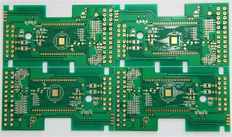
Understanding PCB Etching
Before diving into the specifics of PCB etching, it’s important to understand the fundamentals of the process. PCB etching involves the following key steps:
- Preparing the PCB substrate with a copper layer
- Applying a resist layer to the copper surface
- Exposing the resist layer to UV light through a photomask
- Developing the resist layer to reveal the copper traces
- Etching away the unwanted copper using an etchant solution
- Removing the remaining resist layer to expose the final PCB traces
Each of these steps plays a crucial role in achieving perfect PCB etching, and we will explore them in more detail throughout this article.
Selecting the Right PCB Substrate
The choice of PCB substrate is an important consideration when it comes to achieving perfect etching. The most common substrate materials used in PCB fabrication are:
- FR-4: A flame-retardant fiberglass-reinforced epoxy laminate
- Polyimide: A high-temperature resistant polymer
- Ceramic: A rigid, heat-resistant material used in high-frequency applications
- Aluminum: A metal substrate used for heat dissipation in power electronics
When selecting a PCB substrate, consider factors such as the desired electrical properties, thermal management requirements, and the intended application of the PCB.

Copper Thickness and Quality
The thickness and quality of the copper layer on the PCB substrate also play a significant role in achieving perfect etching. The standard copper thicknesses used in PCB fabrication are:
| Copper Weight (oz/ft²) | Thickness (µm) |
|---|---|
| 0.5 | 17.5 |
| 1 | 35 |
| 2 | 70 |
| 3 | 105 |
Thicker copper layers provide better current-carrying capacity and heat dissipation but can be more challenging to etch accurately. It’s important to select the appropriate copper thickness based on the electrical requirements of your PCB design.
The quality of the copper layer is also crucial for achieving perfect etching. Impurities or defects in the copper can lead to inconsistencies in the etching process, resulting in suboptimal results. Ensure that you source high-quality copper-clad PCB substrates from reputable suppliers.

Photoresist Application Techniques
The photoresist layer is a light-sensitive material that is applied to the copper surface of the PCB substrate. It serves as a protective mask during the etching process, allowing the desired copper traces to remain intact while the unwanted copper is etched away. There are two main types of photoresist used in PCB fabrication:
- Dry film photoresist: A pre-made film that is laminated onto the PCB surface using heat and pressure.
- Liquid photoresist: A liquid material that is spin-coated or sprayed onto the PCB surface and then dried.
Dry film photoresist is often preferred for its ease of use and consistency, while liquid photoresist offers more flexibility in terms of thickness control and conformity to surface irregularities.
When applying the photoresist, it’s crucial to ensure a uniform and defect-free coating. Any air bubbles, dust particles, or other contaminants can lead to imperfections in the final etched PCB. Follow these tips for optimal photoresist application:
- Clean the PCB surface thoroughly before applying the photoresist
- Use a laminator or vacuum laminator for applying dry film photoresist
- Control the spin speed and duration when using liquid photoresist
- Work in a clean, dust-free environment to minimize contamination

Exposure and Development
Once the photoresist is applied, the next step is to expose it to UV light through a photomask. The photomask contains the desired PCB trace pattern, and the UV light selectively hardens the exposed areas of the photoresist.
Proper exposure is critical for achieving sharp, well-defined traces. Factors that influence exposure quality include:
- UV light intensity and wavelength
- Exposure time
- Photomask alignment and contact with the photoresist surface
After exposure, the PCB is developed using a chemical developer solution. The developer dissolves the unexposed areas of the photoresist, revealing the copper traces that will remain after etching. Proper development is essential for ensuring clean, crisp trace edges.
Etching Methods and Etchants
With the photoresist developed, the PCB is ready for etching. There are several methods and etchants used for PCB etching, each with its own advantages and disadvantages.
Ferric Chloride Etching
Ferric chloride (FeCl₃) is a popular etchant for PCB fabrication due to its relatively low cost and ease of use. It is an acidic solution that chemically removes the unwanted copper from the PCB surface.
To use ferric chloride for etching, follow these steps:
- Heat the ferric chloride solution to around 50-60°C (122-140°F) for optimal etching speed
- Immerse the PCB in the heated solution and agitate gently
- Monitor the etching progress and remove the PCB once all the unwanted copper has been etched away
- Rinse the PCB thoroughly with water to remove any residual etchant
While ferric chloride is effective, it can be messy to work with and requires careful disposal due to its corrosive nature.
Cupric Chloride Etching
Cupric chloride (CuCl₂) is another common etchant used in PCB fabrication. It is often used in industrial settings due to its faster etching speed and ability to be regenerated for continuous use.
To use cupric chloride for etching:
- Prepare the cupric chloride solution according to the manufacturer’s instructions
- Heat the solution to around 50-60°C (122-140°F)
- Immerse the PCB in the heated solution and agitate gently
- Monitor the etching progress and remove the PCB once etching is complete
- Rinse the PCB thoroughly with water
Cupric chloride etching typically requires more precise control over the etching parameters compared to ferric chloride, but it can produce excellent results when used correctly.
Spray Etching
Spray etching is a technique that involves spraying the etchant solution onto the PCB surface rather than immersing the board in a tank. This method offers several advantages, including:
- Reduced etchant consumption
- Better control over the etching process
- Improved uniformity and consistency
- Faster etching times
Spray etching systems typically use a motorized spray nozzle to apply the etchant evenly across the PCB surface. The PCB is placed on a conveyor belt or rotating platform to ensure uniform coverage.
When using spray etching, it’s important to optimize the spray pressure, nozzle distance, and etchant temperature to achieve the best results.
Post-Etching Processes
After etching, there are several post-processing steps required to prepare the PCB for the next stages of fabrication.
Resist Stripping
The remaining photoresist layer must be removed from the PCB surface to expose the etched copper traces. This is typically done using a chemical stripper solution specifically designed for removing photoresist.
Follow these steps for resist stripping:
- Immerse the PCB in the stripper solution
- Agitate the solution gently to ensure complete removal of the photoresist
- Rinse the PCB thoroughly with water
- Dry the PCB using compressed air or a clean, lint-free cloth
Tin Plating
After resist stripping, the exposed copper traces can be prone to oxidation and corrosion. To protect the traces and improve solderability, a thin layer of tin is often plated onto the copper surface.
Tin plating can be done using either electroplating or immersion plating techniques. Electroplating involves applying an electrical current to deposit the tin onto the copper, while immersion plating relies on a chemical reaction between the copper and the tin solution.
Solder Mask Application
A solder mask is a protective layer applied to the PCB surface to insulate the copper traces and prevent accidental short circuits during soldering. It also helps to improve the aesthetics of the PCB by providing a uniform color and finish.
Solder mask is typically applied using screen printing or photoimaging techniques. The process involves applying a liquid solder mask material to the PCB surface, curing it using UV light or heat, and then developing the solder mask to expose the desired areas (such as solder pads) for soldering.
Quality Control and Inspection
To ensure perfect PCB etching, it’s crucial to implement robust quality control and inspection procedures throughout the fabrication process. Some key aspects to consider include:
- Visual inspection: Visually examine the PCB for any defects, such as over-etching, under-etching, or trace discontinuities.
- Microscopic inspection: Use a microscope to closely inspect the etched traces for any irregularities or defects.
- Electrical testing: Perform continuity and insulation resistance tests to verify the electrical integrity of the PCB.
- Cross-section analysis: Cut a sample PCB and examine the cross-section under a microscope to evaluate the etching quality and trace dimensions.
By implementing thorough quality control measures, you can identify and correct any issues early in the fabrication process, ensuring the production of perfect etched PCBs.
Frequently Asked Questions (FAQ)
-
What is the best etchant for PCB etching?
The choice of etchant depends on various factors, such as etching speed, cost, and environmental considerations. Ferric chloride and cupric chloride are two commonly used etchants, each with its own advantages and disadvantages. Ultimately, the best etchant for your specific application will depend on your requirements and preferences. -
How long does PCB etching take?
The etching time depends on several factors, including the etchant type, concentration, temperature, and the thickness of the copper layer. Generally, etching can take anywhere from a few minutes to several hours. To minimize etching time while maintaining quality, it’s important to optimize the etching parameters and monitor the process closely. -
Can I reuse the etchant solution?
Some etchants, such as cupric chloride, can be regenerated and reused multiple times. However, the effectiveness of the etchant may diminish over time, and it’s important to monitor the solution’s performance and replace it when necessary. Ferric chloride, on the other hand, is typically disposed of after each use due to the accumulation of copper in the solution. -
What safety precautions should I take when etching PCBs?
PCB etching involves the use of corrosive chemicals and requires proper safety precautions. Always wear appropriate personal protective equipment (PPE), such as gloves, safety glasses, and a lab coat or apron. Work in a well-ventilated area and avoid skin contact or inhalation of the etchant fumes. Properly dispose of used etchant and any contaminated materials in accordance with local regulations. -
Can I etch PCBs at home?
Yes, it is possible to etch PCBs at home using readily available materials and equipment. However, it’s crucial to follow proper safety guidelines and ensure that you have a suitable workspace and ventilation. If you’re new to PCB etching, it’s recommended to start with simple designs and gradually work your way up to more complex projects as you gain experience and confidence in the process.
Conclusion
Achieving perfect PCB etching requires a combination of the right materials, techniques, and processes. By understanding the fundamentals of PCB etching, selecting the appropriate substrate and etchant, and following best practices for photoresist application, exposure, and development, you can create high-quality PCBs with clean, well-defined traces.
Remember to prioritize safety and implement thorough quality control measures to ensure consistent results. With practice and attention to detail, you can master the art of PCB etching and produce professional-grade PCBs for your projects.
No responses yet