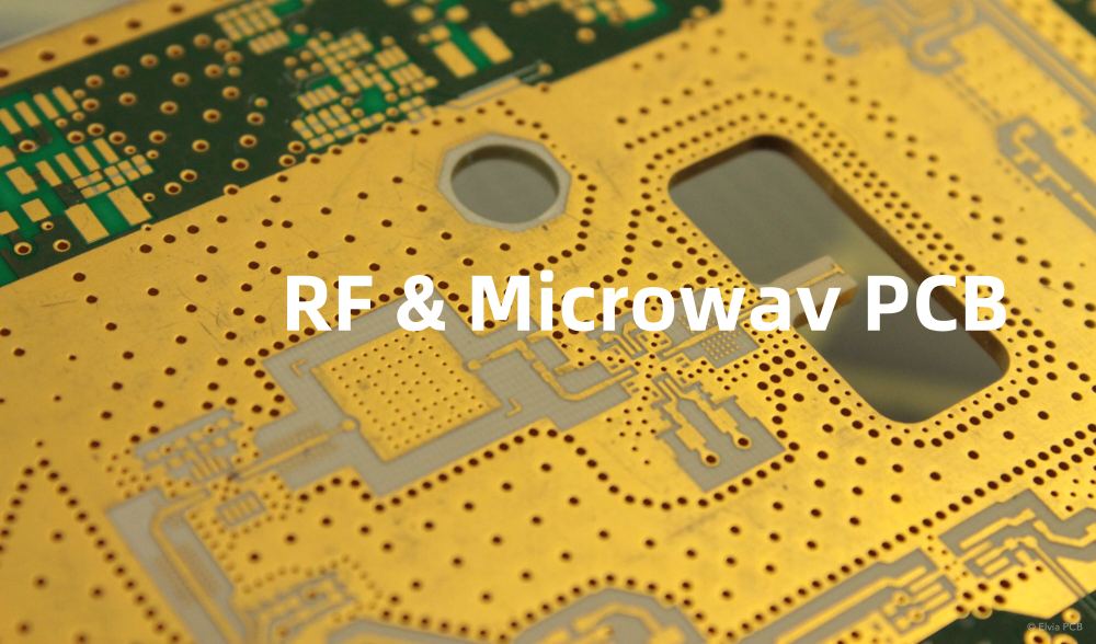
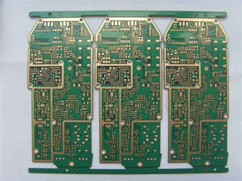
Introduction to Multilayer PCB Boards
Multilayer PCB boards have become increasingly popular in the electronics industry due to their ability to accommodate complex circuits and high component density. These boards consist of multiple layers of conductive material, typically copper, separated by insulating layers. By utilizing multiple layers, designers can create more compact and efficient designs compared to traditional single or double-layer PCBs.
However, as with any technology, multilayer PCB boards have their limitations. These limitations can affect the performance, reliability, and manufacturability of the final product. In this article, we will explore the various limitations of multilayer PCB boards and discuss potential solutions to overcome these challenges.
Limitations of Multilayer PCB Boards
Signal Integrity Issues
One of the primary limitations of multilayer PCB boards is the potential for signal integrity issues. As the number of layers increases, so does the complexity of the board’s electrical characteristics. This complexity can lead to problems such as crosstalk, signal reflections, and electromagnetic interference (EMI).
Crosstalk occurs when signals from one trace interfere with signals on adjacent traces. This interference can cause signal distortion and errors in data transmission. Signal reflections happen when a signal encounters an impedance mismatch, causing a portion of the signal to reflect back towards the source. These reflections can also lead to signal distortion and timing issues.
EMI is another concern with multilayer PCB boards. As the density of components and traces increases, the board becomes more susceptible to both emitting and receiving electromagnetic interference. This interference can cause problems with nearby electronic devices and may violate regulatory standards.
To mitigate these signal integrity issues, designers can employ various techniques:
- Proper layer stackup design: By carefully arranging the layers and choosing appropriate materials, designers can minimize crosstalk and signal reflections.
- Controlled impedance: Maintaining consistent impedance throughout the board can help reduce signal reflections and improve signal quality.
- Shielding and grounding: Incorporating shielding layers and proper grounding techniques can help reduce EMI and improve overall signal integrity.
Thermal Management Challenges
Another limitation of multilayer PCB boards is the challenge of effective thermal management. As the number of layers and component density increases, so does the amount of heat generated within the board. If this heat is not properly dissipated, it can lead to component failure and reduced reliability.
The primary issue with thermal management in multilayer boards is the limited ability for heat to escape from the inner layers. The insulating layers between the conductive layers act as thermal barriers, making it difficult for heat to dissipate efficiently.
To address thermal management challenges, designers can consider the following solutions:
- Thermal vias: Adding thermal vias, which are conductive paths that transfer heat from the inner layers to the outer layers, can improve heat dissipation.
- Heatsinks and cooling solutions: Incorporating heatsinks or other cooling solutions, such as fans or liquid cooling, can help remove heat from the board more effectively.
- Material selection: Choosing materials with good thermal conductivity, such as metal core PCBs or high-performance insulating materials, can improve overall thermal performance.
Manufacturing Complexity and Cost
As the number of layers in a PCB board increases, so does the manufacturing complexity and cost. Each additional layer requires precise alignment, drilling, and lamination processes, which can be time-consuming and expensive.
The increased complexity also leads to a higher risk of manufacturing defects. Even small misalignments or lamination issues can cause problems with the final product, leading to reduced yield and increased costs.
To address manufacturing complexity and cost, designers can consider the following strategies:
- Design for manufacturability (DFM): By following DFM guidelines and considering manufacturing constraints early in the design process, designers can create boards that are easier and more cost-effective to produce.
- Optimize layer count: While adding layers can provide benefits, it’s important to strike a balance between functionality and manufacturability. Designers should aim to use the minimum number of layers necessary to achieve the desired performance.
- Partner with experienced manufacturers: Working with PCB manufacturers who have experience with multilayer boards and advanced manufacturing capabilities can help ensure a smooth and cost-effective production process.
Limitations in Board Size and Thickness
Multilayer PCB boards also face limitations in terms of board size and thickness. As the number of layers increases, the overall thickness of the board also increases. This increased thickness can pose challenges for applications that require slim or compact designs.
Additionally, the maximum board size for multilayer PCBs is typically smaller than that of single or double-layer boards. This limitation is due to the increased complexity of the manufacturing process and the need to maintain precise alignment across all layers.
To work within these limitations, designers can consider the following approaches:
- High-density interconnect (HDI) technology: HDI PCBs use smaller vias and trace widths to achieve higher component density without increasing board size or thickness.
- Flexible and rigid-flex PCBs: Incorporating flexible layers into the board stack-up can help reduce overall thickness and improve conformity to space-constrained applications.
- Modular design: Breaking down a complex design into smaller, interconnected modules can help reduce individual board size and thickness while still achieving the desired functionality.
Overcoming Multilayer PCB Limitations through Advanced Technologies
Despite the limitations of multilayer PCB boards, advancements in technology and manufacturing processes have enabled designers to push the boundaries of what is possible. Some of these advanced technologies include:
High-Density Interconnect (HDI) PCBs
HDI technology involves using smaller vias, narrower traces, and finer pitch components to achieve higher component density and improved electrical performance. By utilizing HDI techniques, designers can create multilayer boards with increased functionality and reduced size.
| Feature | Standard PCB | HDI PCB |
|---|---|---|
| Via Size | 0.3 mm – 0.5 mm | 0.1 mm – 0.15 mm |
| Trace Width | 0.15 mm – 0.2 mm | 0.075 mm – 0.1 mm |
| Pitch | 0.5 mm – 0.8 mm | 0.3 mm – 0.4 mm |
As shown in the table above, HDI PCBs offer significant reductions in via size, trace width, and pitch compared to standard PCBs. These improvements allow for higher component density and more complex designs in a smaller form factor.
Embedded Components
Embedded component technology involves placing components directly within the layers of a multilayer PCB board. This approach can reduce board size, improve electrical performance, and enhance thermal management.
By embedding components, designers can reduce the overall footprint of the board and minimize the distance between components, leading to improved signal integrity and reduced EMI. Additionally, embedded components can be placed closer to the heat-dissipating layers, improving thermal performance.
3D PCBs
3D PCB technology takes the concept of multilayer boards to the next level by allowing designers to create three-dimensional structures. This technology involves stacking and interconnecting multiple PCBs to form a single, compact module.
3D PCBs offer several advantages, including reduced board size, improved signal integrity, and enhanced thermal management. By utilizing the vertical space, designers can create more complex and efficient designs in a smaller form factor.
Advanced Materials
The development of advanced PCB materials has also helped overcome some of the limitations of multilayer boards. These materials offer improved electrical, thermal, and mechanical properties, enabling designers to push the boundaries of performance and reliability.
Some examples of advanced PCB materials include:
- Low-loss dielectrics: These materials offer lower dielectric constant and dissipation factor, reducing signal loss and improving signal integrity at high frequencies.
- High-temperature materials: Materials that can withstand higher operating temperatures enable multilayer boards to be used in more demanding applications, such as automotive and aerospace industries.
- Metal core substrates: These materials combine a metal core with a dielectric layer, providing excellent thermal conductivity and improved thermal management.

FAQ
-
Q: What are the main limitations of multilayer PCB boards?
A: The main limitations of multilayer PCB boards include signal integrity issues, thermal management challenges, manufacturing complexity and cost, and limitations in board size and thickness. -
Q: How can designers mitigate signal integrity issues in multilayer PCBs?
A: Designers can mitigate signal integrity issues by employing proper layer stackup design, controlled impedance, shielding, and grounding techniques. -
Q: What are some strategies for addressing thermal management challenges in multilayer PCBs?
A: Strategies for addressing thermal management challenges include using thermal vias, incorporating heatsinks or cooling solutions, and selecting materials with good thermal conductivity. -
Q: How can designers work within the limitations of board size and thickness in multilayer PCBs?
A: Designers can work within these limitations by utilizing HDI technology, incorporating flexible layers, and adopting a modular design approach. -
Q: What are some advanced technologies that can help overcome the limitations of multilayer PCB boards?
A: Advanced technologies that can help overcome multilayer PCB limitations include HDI PCBs, embedded components, 3D PCBs, and advanced materials with improved electrical, thermal, and mechanical properties.
Conclusion
Multilayer PCB boards have revolutionized the electronics industry by enabling the creation of complex, high-density designs. However, these boards come with their own set of limitations, including signal integrity issues, thermal management challenges, manufacturing complexity, and restrictions on board size and thickness.
Despite these limitations, advancements in technology and manufacturing processes have provided solutions to overcome many of these challenges. By employing techniques such as proper layer stackup design, controlled impedance, thermal management strategies, and advanced technologies like HDI, embedded components, and 3D PCBs, designers can push the boundaries of what is possible with multilayer PCB boards.
As the demand for more complex and compact electronic devices continues to grow, the development of new technologies and materials will be crucial in overcoming the limitations of multilayer PCBs. By staying up-to-date with the latest advancements and working closely with experienced PCB manufacturers, designers can create innovative and reliable multilayer PCB designs that meet the ever-evolving needs of the electronics industry.

No responses yet