What is a PCB Layout?
A PCB (Printed Circuit Board) layout is the design and arrangement of electronic components and the copper traces that connect them on a printed circuit board. The layout is a critical step in the PCB design process, as it determines the functionality, reliability, and manufacturability of the final product.
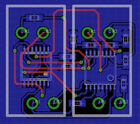
Key Components of a PCB Layout
- Components: The electronic parts that make up the circuit, such as resistors, capacitors, integrated circuits (ICs), and connectors.
- Copper Traces: The conductive paths that connect the components, allowing electrical signals to flow between them.
- Pads: The exposed copper areas where components are soldered to the board.
- Vias: Conductive holes that allow traces to pass from one layer of the PCB to another.
- Silkscreen: The text and symbols printed on the PCB for identification and assembly purposes.
The PCB Layout Design Process
Step 1: Schematic Design
Before creating the PCB layout, you must first design the schematic. The schematic is a graphical representation of the circuit, showing the components and their interconnections. It serves as a blueprint for the PCB layout.
Step 2: Component Placement
Once the schematic is complete, the next step is to place the components on the PCB. Proper component placement is crucial for several reasons:
- Signal Integrity: Components should be placed to minimize the length of critical signal paths and reduce crosstalk.
- Thermal Management: Heat-generating components should be spaced out and placed near the edge of the board for better heat dissipation.
- Mechanical Considerations: Components should be placed to allow for easy assembly and to avoid physical interference.
Step 3: Routing
After the components are placed, the next step is to route the copper traces that connect them. Routing is a complex process that involves several considerations:
- Signal Integrity: Traces should be routed to minimize signal reflections, crosstalk, and electromagnetic interference (EMI).
- Current Capacity: Trace width should be sufficient to handle the expected current flow without excessive heating.
- Manufacturing Constraints: Trace width and spacing must meet the capabilities of the PCB manufacturer.
Step 4: Design Rule Check (DRC)
Once the layout is complete, it must be checked against a set of design rules to ensure manufacturability and reliability. The design rules specify parameters such as:
- Minimum trace width and spacing
- Minimum drill hole size
- Minimum clearance between components and traces
- Maximum number of layers
The DRC process identifies any violations of these rules, allowing the designer to correct them before sending the layout for manufacturing.
Step 5: Gerber File Generation
After the layout passes the DRC, the final step is to generate the Gerber files. Gerber files are the industry-standard format for describing the PCB layout to the manufacturer. They contain all the information needed to fabricate the board, including:
- Copper layers
- Solder mask
- Silkscreen
- Drill holes

PCB Layout Best Practices
To ensure a successful PCB layout, follow these best practices:
1. Keep Signal Paths Short
Minimizing the length of signal paths reduces signal propagation delay, signal reflections, and electromagnetic interference (EMI). This is especially important for high-speed signals.
2. Use Ground Planes
Using a solid ground plane on one or more layers of the PCB provides a low-impedance return path for signals, reduces EMI, and improves signal integrity.
3. Decouple Power Supply
Place decoupling capacitors close to the power pins of ICs to reduce power supply noise and ensure stable operation.
4. Minimize Crosstalk
Crosstalk occurs when signals on adjacent traces interfere with each other. To minimize crosstalk:
- Keep sensitive signals away from noisy signals
- Use guard traces or ground traces between sensitive signals
- Route sensitive signals on different layers
5. Consider Thermal Management
For heat-generating components such as power transistors and voltage regulators, provide adequate copper area for heat dissipation. Use thermal vias to conduct heat to other layers of the board.

Common PCB Layout Mistakes to Avoid
- Incorrect component orientation
- Insufficient clearance between components and traces
- Unconnected traces or pads
- Trace widths too narrow for the expected current
- Inadequate grounding or power supply decoupling

PCB Layout Tools
There are several software tools available for PCB layout design, ranging from free open-source programs to high-end commercial packages. Some popular options include:
| Tool | Vendor | Type |
|---|---|---|
| Eagle | Autodesk | Commercial |
| KiCad | KiCad | Open-Source |
| Altium Designer | Altium | Commercial |
| OrCAD PCB Designer | Cadence | Commercial |
Choose a tool that suits your needs and budget, and invest time in learning its features and capabilities.
Frequently Asked Questions (FAQ)
1. What is the difference between a schematic and a PCB layout?
A schematic is a graphical representation of a circuit’s components and their interconnections, while a PCB layout is the physical arrangement of those components and the copper traces that connect them on a printed circuit board.
2. How do I choose the right trace width for my PCB layout?
Trace width depends on several factors, including the expected current flow, the thickness of the copper layer, and the maximum allowable temperature rise. There are online calculators and tables available to help determine the appropriate trace width for your design.
3. What is a design rule check (DRC), and why is it important?
A design rule check (DRC) is a process of verifying that a PCB layout meets a set of predefined design rules, such as minimum trace width and spacing, minimum drill hole size, and maximum number of layers. The DRC ensures that the layout is manufacturable and reliable.
4. How can I minimize electromagnetic interference (EMI) in my PCB layout?
To minimize EMI, keep signal paths short, use ground planes, route sensitive signals away from noisy signals, and use guard traces or ground traces between sensitive signals. Additionally, consider using shielding techniques such as grounded enclosures or shielding gaskets.
5. What are Gerber files, and why are they important?
Gerber files are the industry-standard format for describing a PCB layout to the manufacturer. They contain all the information needed to fabricate the board, including the copper layers, solder mask, silkscreen, and drill holes. Generating accurate Gerber files is essential for ensuring that the manufactured PCB matches your design intent.
Conclusion
Designing a PCB layout is a complex process that requires knowledge of electronic circuits, signal integrity, thermal management, and manufacturing constraints. By following best practices and using the right tools, you can create reliable, manufacturable PCB layouts that bring your electronic designs to life.
No responses yet