Introduction to IC Packaging
Integrated circuit (IC) packaging is an essential part of modern electronics manufacturing. It involves encasing a semiconductor chip or die in a protective package that allows it to be handled and connected to other components on a printed circuit board (PCB). The package provides electrical connections, heat dissipation, and physical protection for the delicate chip inside.
IC packaging has evolved significantly over the years to keep pace with the increasing complexity and miniaturization of semiconductor devices. Today, there are numerous types of IC packages available, each with its own advantages and applications. Understanding the basics of IC packaging is crucial for anyone involved in electronics design, manufacturing, or procurement.
In this article, we will delve into the world of IC packaging, exploring its history, types, manufacturing processes, and future trends. We will also discuss why IC packaging is so important for the reliability and performance of electronic devices.
History of IC Packaging
The history of IC packaging dates back to the invention of the integrated circuit itself. In 1958, Jack Kilby of Texas Instruments created the first IC by combining multiple transistors on a single germanium substrate. However, this early IC had no package and was connected directly to a PCB using fine gold wires.
In 1959, Robert Noyce of Fairchild Semiconductor developed the first planar IC, which used a silicon substrate and aluminum metallization. This allowed for the creation of more complex circuits and paved the way for mass production of ICs. Noyce also invented the first IC package, which was a ceramic flat pack with leads extending from the sides.
Over the next few decades, IC packaging evolved rapidly to accommodate the increasing complexity and density of semiconductor devices. Some key milestones include:
- 1960s: Development of the dual in-line package (DIP), which became the standard for through-hole mounting of ICs on PCBs.
- 1970s: Introduction of surface-mount technology (SMT) and the small-outline integrated circuit (SOIC) package, which allowed for denser PCB layouts and automated assembly.
- 1980s: Development of pin grid array (PGA) and ball grid array (BGA) packages for high-density ICs with hundreds of pins.
- 1990s: Introduction of chip-scale packages (CSP) and flip-chip technology, which allowed for even smaller package sizes and higher performance.
- 2000s: Development of 3D packaging technologies such as package-on-package (PoP) and through-silicon via (TSV), which enabled stacking of multiple chips in a single package.
Today, IC packaging continues to evolve to meet the demands of emerging technologies such as 5G, artificial intelligence, and the Internet of Things (IoT). New materials, designs, and manufacturing processes are being developed to enable even smaller, faster, and more power-efficient devices.

Types of IC Packages
There are numerous types of IC packages available, each with its own characteristics and applications. Some of the most common types include:
Dual In-Line Package (DIP)
The DIP is one of the oldest and most widely used IC packages. It consists of a rectangular plastic or ceramic package with two parallel rows of pins extending from the sides. DIPs are designed for through-hole mounting on PCBs and are commonly used for low-density ICs such as microcontrollers and memory chips.
Small Outline Integrated Circuit (SOIC)
The SOIC is a surface-mount package that is smaller and thinner than the DIP. It has two rows of pins that are bent to form “gull wings” that can be soldered directly to the surface of a PCB. SOICs are commonly used for medium-density ICs such as op-amps, voltage regulators, and interface chips.
Quad Flat Pack (QFP)
The QFP is a surface-mount package with pins on all four sides of the package. It is available in various sizes and pin counts, ranging from a few dozen to several hundred pins. QFPs are commonly used for high-density ICs such as microprocessors, FPGAs, and ASICs.
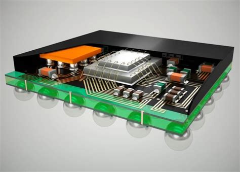
Ball Grid Array (BGA)
The BGA is a surface-mount package with an array of solder balls on the bottom of the package. The balls are used to make electrical connections to the PCB, allowing for a high density of interconnects in a small area. BGAs are commonly used for very high-density ICs such as graphics processors, network processors, and system-on-chip (SoC) devices.
Chip Scale Package (CSP)
The CSP is a small, thin package that is only slightly larger than the die itself. It uses a variety of interconnect technologies, such as wire bonding, flip chip, or through-silicon via (TSV), to connect the die to the package substrate. CSPs are commonly used for space-constrained applications such as mobile devices, wearables, and IoT sensors.
Here is a table summarizing the characteristics of these common IC package types:
| Package Type | Mounting Style | Pin Count | Size | Common Applications |
|---|---|---|---|---|
| DIP | Through-hole | 8-64 | Large | Low-density ICs |
| SOIC | Surface-mount | 8-56 | Medium | Medium-density ICs |
| QFP | Surface-mount | 32-400+ | Medium to Large | High-density ICs |
| BGA | Surface-mount | 100-1000+ | Small to Large | Very high-density ICs |
| CSP | Surface-mount | Varies | Very Small | Space-constrained applications |

IC Packaging Manufacturing Process
The manufacturing process for IC packages involves several steps, which may vary depending on the specific package type and technology used. However, the general process flow is as follows:
-
Wafer Fabrication: The semiconductor devices are fabricated on a silicon wafer using photolithography and other processes. The wafer contains multiple copies of the same device.
-
Wafer Probe: The devices on the wafer are tested using a probe card to identify good and bad die. Bad die are marked with ink dots.
-
Wafer Dicing: The wafer is cut into individual die using a diamond saw or laser cutting tool.
-
Die Attach: The good die are picked up and placed onto a package substrate or leadframe using an automated pick-and-place machine. The die are attached using an adhesive or solder.
-
Wire Bonding: Fine gold or aluminum wires are used to connect the bond pads on the die to the package leads or substrate using a wire bonding machine. This creates the electrical connections between the die and package.
-
Encapsulation: The package is filled with a molding compound, usually a plastic resin, to protect the die and wire bonds from damage and contamination. The molding is done using a transfer molding process.
-
Marking: The package is marked with identifying information such as the device type, manufacturer logo, and date code using laser marking or ink printing.
-
Singulation: The individual packages are separated from the strip or matrix using a saw or punch tool.
-
Final Test: The packaged devices are tested again to ensure they meet the required specifications for functionality, performance, and reliability.
The specific materials and processes used for IC packaging depend on the package type and the requirements of the application. For example, high-performance devices may require advanced packaging technologies such as flip chip or 3D packaging to achieve the necessary speed, power, and density.

Importance of IC Packaging
IC packaging plays a critical role in the performance, reliability, and cost of electronic devices. Some of the key reasons why IC packaging is so important include:
Electrical Connections
The primary function of an IC package is to provide electrical connections between the semiconductor die and the PCB. The package leads or pins are designed to match the PCB layout and provide a reliable, low-resistance path for signals and power to flow between the die and other components on the board.
Physical Protection
The package also provides physical protection for the delicate semiconductor die, which is typically only a few millimeters in size and very fragile. The package encapsulates the die in a robust, moisture-resistant material that can withstand handling, vibration, and other environmental stresses.
Thermal Management
Semiconductor devices generate heat during operation, and this heat must be dissipated to prevent damage or degradation of performance. The package plays a key role in thermal management by providing a path for heat to flow from the die to the PCB or heatsink. Some packages also include features such as thermal vias or heat spreaders to enhance heat dissipation.
Mechanical Support
The package provides mechanical support for the die during handling, testing, and assembly. This is especially important for larger or heavier die that may be prone to cracking or damage if not properly supported.
Cost Reduction
IC packaging also plays a role in reducing the overall cost of electronic devices. By standardizing package sizes and layouts, manufacturers can achieve economies of scale and reduce the cost of packaging materials and assembly processes. Advanced packaging technologies such as 3D packaging and wafer-level packaging can also help reduce the size and cost of devices by integrating multiple functions into a single package.
Future Trends in IC Packaging
As electronic devices continue to become smaller, faster, and more complex, IC packaging technology must also evolve to keep pace. Some of the key trends and developments in IC packaging include:
Advanced Materials
New materials such as high-density interconnect (HDI) substrates, low-K dielectrics, and advanced molding compounds are being developed to enable smaller, faster, and more reliable packages.
3D Packaging
3D packaging technologies such as package-on-package (PoP) and through-silicon via (TSV) are becoming increasingly popular for high-density applications such as mobile devices and AI accelerators. These technologies allow multiple chips to be stacked vertically in a single package, reducing size and improving performance.
Wafer-Level Packaging
Wafer-level packaging (WLP) is a technology that allows the entire wafer to be packaged before dicing, reducing the size and cost of the final package. WLP is particularly well-suited for small, low-cost devices such as sensors and RF components.
Heterogeneous Integration
Heterogeneous integration refers to the combining of multiple different devices, such as processors, memory, sensors, and RF components, into a single package. This allows for more complex and diverse functionality in a smaller form factor, enabling new applications such as wearables and IoT devices.
Advanced Testing
As packages become more complex and diverse, new testing technologies are needed to ensure reliability and performance. Techniques such as built-in self-test (BIST), 3D X-ray imaging, and advanced thermal analysis are being developed to enable faster and more comprehensive testing of packaged devices.
Frequently Asked Questions
What is the difference between an IC package and a chip?
An IC package is the protective enclosure that contains the semiconductor chip or die. The chip is the actual device that performs the electronic functions, while the package provides the necessary electrical connections, physical protection, and thermal management to allow the chip to operate reliably.
What is the most common type of IC package?
The most common type of IC package depends on the application and the era. Historically, the dual in-line package (DIP) was the most widely used package for through-hole mounting of ICs. Today, surface-mount packages such as the small-outline integrated circuit (SOIC) and quad flat pack (QFP) are more common for medium- to high-density applications.
What is the smallest type of IC package?
The smallest types of IC packages are chip-scale packages (CSPs) and wafer-level packages (WLPs). These packages are only slightly larger than the semiconductor die itself and are designed for space-constrained applications such as mobile devices and IoT sensors.
What materials are used in IC packages?
IC packages can be made from a variety of materials, depending on the specific requirements of the application. Common materials include:
- Plastics such as epoxy resins for molding compounds and substrates
- Ceramics such as alumina for high-reliability packages
- Metals such as copper for leadframes and heat spreaders
- Composites such as bismaleimide triazine (BT) for high-density substrates
How long does it take to package an IC?
The time required to package an IC depends on the specific package type and manufacturing process used. In general, the packaging process can take anywhere from a few minutes to several hours per device, depending on the complexity of the package and the volume of production. Advanced packaging technologies such as 3D packaging and wafer-level packaging can help reduce the time and cost of packaging by allowing multiple devices to be packaged simultaneously.
Conclusion
IC packaging is a critical aspect of modern electronics manufacturing that enables the reliable and efficient operation of semiconductor devices in a wide range of applications. From the earliest ceramic flat packs to the latest 3D and wafer-level packages, IC packaging technology has evolved to keep pace with the increasing complexity and miniaturization of electronic devices.
Understanding the basics of IC packaging, including the different types of packages, manufacturing processes, and future trends, is essential for anyone involved in electronics design, manufacturing, or procurement. By selecting the appropriate package type and technology for a given application, designers can optimize the performance, reliability, and cost of their products.
As electronic devices continue to become smaller, faster, and more complex, IC packaging will play an increasingly important role in enabling new applications and technologies. From 5G smartphones to AI-powered robots to IoT sensors, the future of electronics will depend on the continued innovation and advancement of IC packaging technology.
No responses yet