Introduction to 10-Layer PCBs and PCB Fabrication
10-layer printed circuit boards (PCBs) are complex, high-density boards used in advanced electronics applications that require a large number of interconnections and signal routing in a compact form factor. The 10 conductive layers allow for an extremely high level of circuit integration and functionality compared to simpler 2-layer or 4-layer boards.
PCB fabrication is the process of manufacturing printed circuit boards. It involves a series of steps to build up the layers of conductive copper traces and insulating substrate material, drill holes, plate vias to interconnect the layers, apply solder mask and silkscreen, and cut out the individual boards from the panel.
Achieving high quality, reliable 10-layer PCBs requires careful design, material selection, and precision manufacturing processes from an experienced PCB fabrication partner. In this article, we’ll dive into the key aspects of 10-layer PCB fabrication and provide tips on how to get the best boards for your next project.
Advantages and Applications of 10-Layer PCBs
Benefits of High Layer Count Boards
Using a 10-layer PCB provides several important benefits over boards with fewer layers:
- Smaller form factor and higher component density
- Improved signal integrity and reduced crosstalk
- Better power distribution and thermal management
- Increased reliability and reduced EMI/RFI issues
By using 10 conductive layers, designers can route a large number of signals and power traces in a compact area. The additional layers also allow for dedicated power and ground planes that provide shielding between signal layers to minimize crosstalk and EMI.
10-Layer PCB Applications
The high density and performance of 10-layer PCBs make them well-suited for a range of demanding electronics applications, such as:
- High-speed digital systems (e.g. networking equipment, servers, GPUs)
- RF and wireless communication devices
- Medical and scientific instrumentation
- Aerospace and defense systems
- High-end consumer electronics
In these applications, 10-layer PCBs enable advanced capabilities and functionality while meeting strict size, weight, and reliability requirements. However, the complexity of these boards also necessitates careful PCB fabrication processes to ensure they perform as intended.

10-Layer PCB Stackup and Materials
Typical 10-Layer Board Stackup
The layer stackup refers to the arrangement of conductive and insulating layers in a PCB. A typical 10-layer PCB stackup consists of the following layers:
| Layer | Type | Thickness (mils) |
|---|---|---|
| 1 | Signal | 1.4 |
| 2 | Ground | 1.4 |
| 3 | Signal | 1.2 |
| 4 | Signal | 1.2 |
| 5 | Power | 1.2 |
| 6 | Signal | 1.2 |
| 7 | Signal | 1.2 |
| 8 | Ground | 1.4 |
| 9 | Signal | 1.4 |
| 10 | Signal | 1.4 |
The signal layers are used for routing traces between components. The power layers distribute voltage to the components. The ground layers provide a reference plane and shielding. Insulating dielectric material separates the conductive layers.
Choosing the Right PCB Materials
Selecting the appropriate PCB materials is critical for 10-layer fabrication. Key considerations include:
- Laminate material (FR-4, high-Tg, etc.)
- Copper foil weight and type
- Solder mask color and finish
- Silkscreen legend ink color
- Surface finish (HASL, ENIG, IAg, etc.)
For high-speed designs, using low-loss, high-Tg laminates like Isola 370HR or Rogers 4000 series can minimize signal integrity issues. Careful stackup planning and impedance control are also important.
Your PCB fabrication partner can help recommend the best materials for your specific 10-layer design and performance requirements. Be sure to also consider lead times and costs when making material choices.

10-Layer PCB Design Considerations
Avoiding Common Pitfalls
Designing a 10-layer PCB is significantly more complex than simpler 2 or 4 layer boards. Common pitfalls to avoid include:
- Overly dense component placement and routing
- Insufficient via spacing and hole-to-copper clearance
- Incorrect plane assignments and reference designators
- Mismatched controlled impedance traces
- Inadequate thermal relief and copper balancing
Work closely with your PCB design and fabrication teams to carefully review your 10-layer designs before manufacturing. Use DFM analysis tools to check for any potential issues.
Signal Integrity and Power Delivery
Maintaining signal integrity and proper power delivery are critical for 10-layer PCBs running at high speeds. Some key considerations:
- Route high-speed signals on inner layers between reference planes
- Avoid daisy-chaining vias and use stitching vias for long traces
- Size power planes appropriately for current loads
- Use sufficient decoupling capacitors near ICs
- Simulate and verify stackup impedance and crosstalk
Proper layout techniques, stackup design, and simulation can help identify and mitigate signal integrity and power delivery issues early in the design phase. Engage with your fabrication partner for a design review.

PCB Fabrication Process Steps
Overview of 10-Layer Manufacturing Flow
Fabricating a 10-layer PCB involves a series of complex process steps:
- Material preparation and inner layer printing
- Inner layer etching and AOI
- Lamination and drilling
- Desmear and electroless copper deposition
- Pattern plating and outer layer etching
- Solder mask application and curing
- Surface finish and silkscreen legend
- Electrical test and final inspection
Each step must be tightly controlled to achieve the required feature sizes, tolerances, and reliability for 10-layer boards. Experienced PCB fabrication engineers oversee the entire process flow.
Critical Process Control Points
There are several critical process steps that require special attention during 10-layer PCB fabrication:
- Registration and alignment of inner layers during lamination
- Drilling and plating of high aspect ratio vias
- Etching of fine pitch traces and spaces
- Application and curing of solder mask to prevent defects
- Control of surface finish thickness and coverage
Careful process control and monitoring at these steps is essential to producing high-quality 10-layer boards. Look for a PCB fabrication partner with a robust quality management system and experienced engineering team.
Ensuring 10-Layer PCB Quality and Reliability
Testing and Inspection Methods
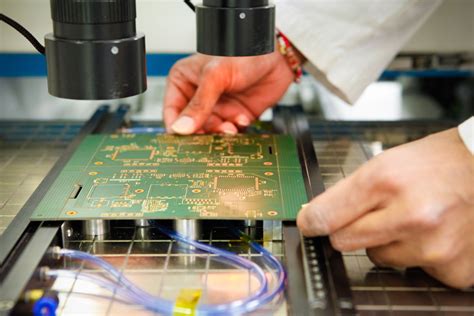
Thorough testing and inspection are critical for ensuring the quality and reliability of manufactured 10-layer PCBs. Common methods include:
- Automated optical inspection (AOI) of inner layers and outer layers
- Microsection analysis of vias and plating thickness
- Electrical testing for opens and shorts (flying probe or bed of nails)
- Impedance testing of controlled traces
- Visual inspection for workmanship defects
Your PCB fabrication partner should have a comprehensive test and inspection plan that covers all aspects of the board. Review their quality control procedures and reporting.
Reliability Testing and Qualifications
For critical applications, additional reliability testing may be required to validate the long-term performance of 10-layer PCBs. Some common qualifications include:
- Thermal cycling and shock testing
- Highly accelerated life testing (HALT)
- Vibration and mechanical shock testing
- Moisture sensitivity and salt spray testing
- Interconnect stress testing (IST)
Work with your fabrication partner to determine which reliability tests are needed based on your end-use environment and product lifetime requirements. Factor in additional time and cost for these qualifications.
How to Select a 10-Layer PCB Fabrication Partner
Key Evaluation Criteria
Choosing the right PCB fabrication partner is essential for successfully manufacturing high-quality 10-layer boards. Some key factors to consider:
- Technical capabilities and equipment for 10-layer fabrication
- Experience with similar designs and industries
- Quality certifications (ISO 9001, IATF 16949, AS9100, etc.)
- Prototype and production volumes and lead times
- Pricing and total cost of ownership
- Customer support and communication
Look for a fabricator with a proven track record of manufacturing complex 10-layer PCBs and expertise in your specific application area. Evaluate multiple potential partners and get references.
Questions to Ask Potential Fabricators
When evaluating potential 10-layer PCB fabrication partners, be sure to ask detailed questions about their capabilities and processes:
- What materials and surface finishes do you support for 10-layer boards?
- What are your standard and minimum feature sizes and tolerances?
- How do you control registration and alignment of inner layers?
- What type of electrical testing and inspection do you perform?
- How do you handle non-conforming products and corrective actions?
- What are your typical lead times and pricing for 10-layer prototypes and production?
The fabricator’s responses will give you insight into their technical expertise, quality focus, and customer service. An experienced, transparent 10-layer PCB manufacturer will be able to address your specific needs.
10-Layer PCB Fabrication FAQs
What is the typical cost of a 10-layer PCB?
The cost of a 10-layer PCB can vary widely depending on factors such as board size, material, surface finish, testing requirements, and order volume. In general, a small prototype run of 10-layer boards may cost several hundred dollars each, while high-volume production pricing may be less than $100 per board. Consult with your PCB fabrication partner for detailed quotes based on your specific design and requirements.
How long does 10-layer PCB fabrication take?
Lead times for 10-layer PCB fabrication depend on the complexity of the design, materials, testing requirements, and manufacturer capacity. Typical prototype lead times range from 2-3 weeks, while production orders may take 4-6 weeks or more. Expedited options may be available for a premium. Provide your PCB fabricator with clear requirements and work closely with them to ensure on-time delivery.
What are the most common 10-layer PCB defects?
Some of the most common defects encountered in 10-layer PCB fabrication include:
- Misregistration or misalignment of layers
- Laminate voids or delamination
- Plating voids or cracks in vias
- Over-etching or under-etching of traces
- Solder mask defects (blisters, cracks, etc.)
Working with an experienced PCB fabricator with robust process controls and inspection procedures can minimize the risk of these defects. Proper design techniques and close collaboration with your manufacturing partner are also essential.
Can 10-layer PCBs be manufactured as flex or rigid-flex?
Yes, 10-layer PCBs can be manufactured as flexible or rigid-flex constructions in addition to standard rigid boards. Flex and rigid-flex 10-layer boards use similar materials and processes but require additional considerations for bend radius, stiffener design, and assembly. They offer unique advantages for applications requiring high density interconnects in three-dimensional configurations. Discuss your flex PCB needs with a fabricator experienced in these advanced technologies.
What file formats are needed for 10-layer PCB fabrication?
PCB fabrication partners typically require a complete set of design files including:
- Gerber files for each conductive layer (.gbr)
- NC drill files (.drl, .ncd)
- Solder mask and silkscreen files (.gbs, .gbo, .gto, .gts)
- Fabrication drawing with notes and specifications (.pdf)
- Bill of Materials (BOM) and component placement file (.xls, .csv)
- 3D CAD model (STEP, IGES) if available
Providing complete, accurate design files in industry-standard formats helps ensure a smooth fabrication process and minimizes delays. Consult with your fabrication partner for their specific requirements and guidelines.
Conclusion
10-layer PCB fabrication is a complex process that requires careful design, material selection, process control, and testing to achieve high-quality, reliable boards. By understanding the key considerations and working closely with an experienced manufacturing partner, you can successfully bring your advanced 10-layer designs to life.
When selecting a 10-layer PCB fabricator, prioritize technical capabilities, quality focus, and customer service. Look for a partner with expertise in your specific application who can provide guidance and support throughout the design and manufacturing process.
With the right approach and partnerships, 10-layer PCBs can enable new levels of performance and innovation in a wide range of demanding electronics applications. As technologies continue to advance, the capabilities of these complex circuit boards will only continue to expand.
No responses yet