Introduction to KiCad
KiCad is a free and open-source software suite for electronic design automation (EDA). It facilitates the design of schematics for electronic circuits and their conversion to PCB designs. KiCad is a cross-platform tool that runs on Windows, Linux, and macOS operating systems.
In this comprehensive KiCad Tutorial, we will guide you through the process of designing a simple PCB using KiCad. By the end of this tutorial, you will have a solid understanding of KiCad’s basic features and workflows.
Getting Started with KiCad
Installing KiCad
To begin, you need to download and install KiCad on your computer. Visit the official KiCad website (https://www.kicad.org/) and download the appropriate version for your operating system. Follow the installation instructions provided on the website.
KiCad Interface Overview
Upon launching KiCad, you will be greeted with the main window. The KiCad interface consists of several key components:
- Project Manager: This is the main window where you manage your projects and access various tools.
- Schematic Editor: Used for creating and editing schematic diagrams of electronic circuits.
- PCB Editor: Allows you to design the physical layout of your PCB.
- Footprint Editor: Enables you to create and edit footprints (component layouts) for your PCB.
- 3D Viewer: Provides a three-dimensional preview of your PCB design.

Creating a New Project
To start a new project in KiCad, follow these steps:
- In the Project Manager, click on “File” > “New Project.”
- Choose a location for your project and give it a name.
- Click “Save” to create the project.
KiCad will create a new project directory with several files, including the project file (.pro) and the schematic file (.sch).

Designing the Schematic
Creating a Schematic
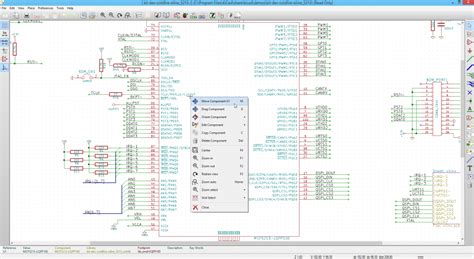
Double-click on the schematic file (.sch) in the Project Manager to open the Schematic Editor. In the Schematic Editor, you will design the electronic circuit using various components and connections.
Adding Components
To add components to your schematic:
- Click on the “Place symbol” button in the toolbar or press the “A” key.
- In the component library browser, search for the desired component and select it.
- Click on the schematic canvas to place the component.
- Repeat the process to add all the necessary components.
Wiring Components
To connect the components in your schematic:
- Click on the “Place wire” button in the toolbar or press the “W” key.
- Click on the first component pin you want to connect.
- Move the cursor to the second component pin and click to create the connection.
- Continue connecting all the required components.
Labeling and Annotating
To improve the readability of your schematic, you can add labels and annotations:
- Click on the “Place text” button in the toolbar or press the “T” key.
- Click on the schematic canvas where you want to place the label or annotation.
- Type the desired text and press Enter.
Saving and Validating the Schematic
Once you have completed your schematic design:
- Click on “File” > “Save” to save your schematic.
- Click on “Tools” > “Electrical Rules Check” to validate your schematic for any errors or warnings.

PCB Design
Creating a PCB Layout
With the schematic design complete, you can now generate the PCB layout:
- Click on “Tools” > “Update PCB from Schematic” to synchronize the schematic with the PCB layout.
- In the Project Manager, double-click on the PCB file (.kicad_pcb) to open the PCB Editor.
Placing Components
In the PCB Editor, you will see the components from your schematic placed on the PCB canvas. To arrange the components:
- Click and drag the components to their desired locations on the PCB.
- Use the “Move” tool (M) to fine-tune the component placement.
Routing Traces
To connect the components on the PCB, you need to route traces:
- Click on the “Route tracks” button in the toolbar or press the “X” key.
- Click on the starting pad of a connection.
- Move the cursor to the ending pad and click to create the trace.
- Repeat the process to route all the necessary connections.
Adding Footprints
Footprints define the physical layout of components on the PCB. To assign footprints to components:
- In the PCB Editor, right-click on a component and select “Properties.”
- In the component properties window, select the appropriate footprint from the library.
- Repeat the process for all components.
Design Rule Checking (DRC)
Before finalizing your PCB design, it’s important to run a Design Rule Check (DRC) to ensure it meets the manufacturing requirements:
- Click on “Tools” > “DRC” to open the DRC window.
- Configure the DRC settings according to your PCB manufacturer’s specifications.
- Click “Run DRC” to check for any design rule violations.
- Address any issues identified by the DRC.
Generating Gerber Files
Gerber files are the industry-standard format for PCB manufacturing. To generate Gerber files:
- Click on “File” > “Plot” to open the Plot window.
- Select the desired layers to include in the Gerber files.
- Configure the plot settings according to your manufacturer’s requirements.
- Click “Plot” to generate the Gerber files.
- Save the Gerber files in a zip archive for submission to the PCB manufacturer.
FAQ
-
Q: Is KiCad suitable for beginners?
A: Yes, KiCad is a great choice for beginners. It offers a user-friendly interface and extensive documentation to help you get started with PCB design. -
Q: Can KiCad be used for complex PCB designs?
A: Absolutely! KiCad is capable of handling both simple and complex PCB designs. It provides a wide range of features and tools to accommodate various design requirements. -
Q: Is KiCad compatible with other EDA software?
A: KiCad supports industry-standard file formats, such as Gerber and ODB++, which allows for compatibility with other EDA software and PCB manufacturers. -
Q: Can I create custom components in KiCad?
A: Yes, KiCad allows you to create custom components using the Symbol Editor and Footprint Editor. You can design your own symbols and footprints to suit your specific needs. -
Q: Is there a community support for KiCad?
A: Yes, KiCad has a large and active community of users and developers. You can find support, resources, and tutorials on the official KiCad forums, as well as on various online platforms and social media groups.
Conclusion
Congratulations! You have completed this KiCad tutorial for beginners. By following the step-by-step guide, you should now have a basic understanding of how to design a PCB using KiCad. Remember to practice regularly and explore the advanced features of KiCad to further enhance your PCB design skills.
KiCad is a powerful and versatile tool that empowers electronic enthusiasts and professionals to create high-quality PCBs. With its open-source nature and active community support, KiCad continues to evolve and improve, making it an excellent choice for your electronic design projects.
Happy PCB designing with KiCad!
No responses yet