Introduction to PCB Manufacture
Printed Circuit Boards (PCBs) are essential components in modern electronics. They provide a platform for mounting and interconnecting electronic components, enabling the creation of complex circuits and devices. In this comprehensive guide, we will walk you through the step-by-step process of PCB manufacture, from design to final assembly.
What is a PCB?
A PCB is a flat board made of insulating material, such as fiberglass or plastic, with conductive copper traces printed on its surface. These traces form the electrical connections between components mounted on the board. PCBs come in various sizes, shapes, and layers, depending on the complexity of the circuit and the intended application.
Advantages of PCBs
PCBs offer several advantages over traditional point-to-point wiring:
- Compact size: PCBs allow for a much smaller and more compact design compared to traditional wiring methods.
- Reliability: The fixed layout of a PCB ensures consistent connections and reduces the risk of short circuits or loose connections.
- Mass production: PCBs can be easily mass-produced, reducing manufacturing costs and time.
- Ease of repair: With a well-designed PCB, it is easier to identify and replace faulty components.
PCB Design
The first step in PCB manufacture is designing the circuit board. This involves creating a schematic diagram and a layout of the components and traces.
Schematic Design
A schematic diagram is a graphical representation of the electronic circuit. It uses standardized symbols to represent components and shows how they are interconnected. The schematic is created using Electronic Design Automation (EDA) software, such as KiCad, Eagle, or Altium Designer.
PCB Layout
Once the schematic is complete, the next step is to create the PCB layout. This involves arranging the components and routing the traces on the board. The layout must consider factors such as component size, trace width, spacing, and layer stackup. EDA software is used to create the layout, which can then be exported as Gerber files for manufacturing.
PCB Fabrication
With the design complete, the next stage is PCB fabrication. This involves several steps to transform the design into a physical board.
Material Selection
The choice of PCB material depends on the application and the required properties, such as thermal conductivity, dielectric constant, and mechanical strength. Common materials include:
- FR-4: A glass-reinforced epoxy laminate, widely used for general-purpose PCBs.
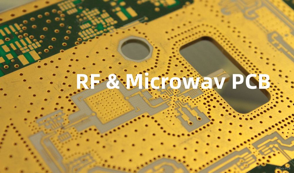
- Rogers: High-frequency laminates with low dielectric loss, used for RF and microwave applications.
- Polyimide: Flexible substrates for applications requiring bendable or rollable PCBs.
Copper Clad Laminate
The base material for a PCB is a copper-clad laminate (CCL). It consists of a thin layer of copper foil bonded to the insulating substrate material. The copper thickness is typically specified in ounces per square foot (oz/ft²), with common thicknesses being 0.5 oz/ft², 1 oz/ft², and 2 oz/ft².
Drilling
Holes are drilled in the CCL to accommodate through-hole components and vias. The drilling process uses high-speed drill bits to create precise holes based on the Gerber drill files generated from the PCB layout. Modern PCB fabrication often employs Computer Numerical Control (CNC) drilling machines for accurate and efficient drilling.
Patterning
The next step is to create the copper trace pattern on the PCB. This is achieved through a process called photolithography. A photosensitive resist is applied to the copper surface, and the desired pattern is transferred using UV light exposure through a photomask. The exposed areas of the resist are then developed and removed, leaving the copper traces protected.
Etching
The unprotected copper areas are removed through a chemical etching process. The most common etchant is ferric chloride, which selectively dissolves the exposed copper while leaving the protected traces intact. After etching, the remaining photoresist is stripped away, revealing the final copper pattern.
Soldermask Application
A soldermask is a protective layer applied to the PCB surface, leaving only the exposed pads and vias for soldering. The soldermask helps prevent solder bridges and provides insulation between adjacent traces. It is typically applied using a silkscreen printing process and then cured using UV light.
Silkscreen
The silkscreen layer is used to add text, logos, and component identifiers to the PCB surface. It is applied using a similar process to the soldermask, with the desired artwork printed using ink on top of the soldermask.
Surface Finish
The exposed copper pads and vias require a surface finish to protect against oxidation and enhance solderability. Common surface finishes include:
- HASL (Hot Air Solder Leveling): A tin-lead alloy is applied to the exposed copper, creating a smooth, solderable surface.
- ENIG (Electroless Nickel Immersion Gold): A thin layer of nickel is deposited, followed by a thin layer of gold, providing excellent solderability and shelf life.
- OSP (Organic Solderability Preservative): A thin, organic coating is applied to the copper, protecting it from oxidation and ensuring good solderability.

PCB Assembly
With the fabricated PCB in hand, the final stage is to assemble the components onto the board.
Component Placement
The components are placed on the PCB according to the assembly drawing, which specifies their locations and orientations. Surface mount components are placed using pick-and-place machines, while through-hole components are inserted manually or with the aid of insertion machines.
Soldering
The components are then soldered to the PCB. For surface mount components, solder paste is applied to the pads using a stencil, and the components are placed on top. The board is then heated in a reflow oven, melting the solder and creating a permanent connection. Through-hole components are soldered using wave soldering or manual soldering techniques.
Inspection and Testing
After assembly, the PCB undergoes visual inspection and electrical testing to ensure proper functionality. Automated optical inspection (AOI) systems can check for correct component placement and soldering quality. Electrical tests, such as in-circuit testing (ICT) or functional testing, verify the circuit’s performance against the design specifications.
Frequently Asked Questions (FAQ)
-
What is the difference between a single-layer and a multi-layer PCB?
A Single-layer PCB has conductive traces on only one side of the board, while a multi-layer PCB has traces on both sides and additional internal layers. Multi-layer PCBs offer higher component density and better signal integrity but are more complex and expensive to manufacture. -
What is the purpose of vias in a PCB?
Vias are small holes drilled through the PCB that allow electrical connections between different layers of the board. They are used to route signals and power between components on different layers, enabling more compact and efficient designs. -
What is the difference between SMD and through-hole components?
Surface Mount Devices (SMDs) are mounted directly onto the surface of the PCB, while through-hole components have leads that are inserted into holes drilled in the board. SMDs are smaller and allow for higher component density, while through-hole components offer better mechanical stability and are easier to hand-solder. -
What is the role of solder paste in PCB assembly?
Solder paste is a mixture of tiny solder particles suspended in a flux medium. It is applied to the pads on the PCB prior to component placement. When heated in a reflow oven, the solder melts and forms a permanent electrical and mechanical connection between the component leads and the pads. -
What are the common causes of PCB failure?
PCB failures can arise from various factors, including: - Manufacturing defects, such as incorrect component placement or poor soldering
- Environmental factors, such as exposure to moisture, heat, or vibration
- Electrical overstress, such as voltage spikes or electrostatic discharge (ESD)
- Mechanical stress, such as bending or impact damage
- Component failure due to aging or quality issues
Proper design, manufacturing, and handling practices can help minimize the risk of PCB failures.
Conclusion
PCB manufacture is a complex process that involves multiple stages, from design to assembly. By understanding the steps involved and the key considerations at each stage, you can ensure the successful creation of reliable and high-quality PCBs for your electronic projects. As technology advances, PCB manufacturing techniques continue to evolve, enabling the development of even more sophisticated and compact electronic devices.
| Step | Description |
|---|---|
| Design | Create schematic and PCB layout using EDA software |
| Material Selection | Choose appropriate PCB material based on application requirements |
| Drilling | Drill holes for through-hole components and vias |
| Patterning | Transfer copper trace pattern using photolithography |
| Etching | Remove unprotected copper using chemical etching |
| Soldermask Application | Apply protective soldermask layer |
| Silkscreen | Add text, logos, and component identifiers |
| Surface Finish | Apply surface finish to protect exposed copper and enhance solderability |
| Component Placement | Place components on the PCB according to assembly drawing |
| Soldering | Solder components using reflow or wave soldering techniques |
| Inspection and Testing | Perform visual inspection and electrical testing to ensure functionality |
By following these steps and understanding the intricacies of PCB manufacture, you can create high-quality, reliable PCBs for your electronic projects.

No responses yet