Introduction to ICT-PCB
In-Circuit Testing (ICT) is a crucial process in the manufacturing of high-quality Printed Circuit Boards (PCBs). It is an automated testing method that verifies the functionality and quality of PCBs by testing each component on the board individually. ICT-PCB testing ensures that the PCB is free from defects such as short circuits, open circuits, and incorrect component placement, which can lead to product failure and customer dissatisfaction.
Benefits of ICT-PCB Testing
- Early detection of defects
- Improved product quality
- Reduced manufacturing costs
- Faster time-to-market
- Enhanced customer satisfaction
The ICT-PCB Testing Process
Preparing the PCB for Testing
Before the ICT-PCB testing process can begin, the PCB must be prepared. This involves several steps:
- Cleaning the PCB to remove any contaminants
- Applying solder paste to the PCB pads
- Placing components on the PCB using a pick-and-place machine
- Soldering the components to the PCB using a reflow oven
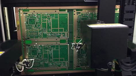
Setting Up the ICT Fixture
Once the PCB is prepared, it is placed into an ICT fixture. The fixture is a custom-designed tool that holds the PCB in place and provides electrical contact points for testing. The fixture is designed to match the specific layout and components of the PCB being tested.
Running the ICT Test
With the PCB securely placed in the ICT fixture, the testing process can begin. The ICT machine applies electrical signals to the contact points on the fixture, which are then transmitted to the corresponding points on the PCB. The machine measures the electrical characteristics of each component on the board, such as resistance, capacitance, and inductance, and compares them to the expected values.
Analyzing the Test Results
After the ICT test is complete, the machine generates a report that details the results of the test. The report includes information on any defects or anomalies detected during the test, such as:
- Short circuits
- Open circuits
- Incorrect component values
- Missing components
- Reversed polarity components
The test results are analyzed by a technician who determines whether the PCB passes or fails the test. If the PCB fails, the technician may perform additional tests or inspections to identify the root cause of the failure.

Common Defects Detected by ICT-PCB Testing
ICT-PCB testing can detect a wide range of defects that can affect the functionality and reliability of the PCB. Some of the most common defects include:
Short Circuits
A short circuit occurs when two or more points on the PCB that should not be connected are accidentally connected. This can happen due to a variety of reasons, such as:
- Solder bridges between adjacent pads
- Conductive debris on the PCB surface
- Damaged or misaligned components
Short circuits can cause the PCB to malfunction or even damage other components on the board.
Open Circuits
An open circuit occurs when there is a break in the electrical path between two points on the PCB that should be connected. This can happen due to:
- Broken or damaged traces on the PCB
- Missing or damaged components
- Poor solder joints
Open circuits can prevent the PCB from functioning properly or cause intermittent issues.
Incorrect Component Values
ICT-PCB testing can detect when a component on the PCB has an incorrect value, such as:
- Wrong resistor or capacitor value
- Incorrect inductance value
- Wrong transistor or diode type
Incorrect component values can cause the PCB to perform poorly or not at all.
Component Defects
ICT-PCB testing can also detect defects in individual components on the PCB, such as:
- Shorted or open pins on an integrated circuit
- Damaged or missing leads on a component
- Incorrect orientation of a component
Component defects can cause the PCB to malfunction or fail prematurely.

Best Practices for ICT-PCB Testing
To ensure the best results from ICT-PCB testing, there are several best practices that should be followed:
Design for Testability
When designing a PCB, it is important to consider testability from the beginning. This means designing the PCB layout and component placement in a way that facilitates easy testing with an ICT fixture. Some best practices for designing for testability include:
- Providing test points on the PCB for critical signals
- Avoiding dense component placement that makes testing difficult
- Using standard component packages and footprints
Use High-Quality Components
Using high-quality components can help reduce the likelihood of defects and improve the overall reliability of the PCB. When sourcing components, it is important to choose reputable suppliers and verify the quality of the components through testing and inspection.
Implement Proper Handling and Storage Procedures
Proper handling and storage procedures can help prevent damage to PCBs and components during the manufacturing process. This includes:
- Using electrostatic discharge (ESD) protection when handling PCBs and components
- Storing PCBs and components in a clean, dry environment
- Avoiding exposure to extreme temperatures or humidity
Regularly Maintain and Calibrate Test Equipment
Regular maintenance and calibration of test equipment is essential for ensuring accurate and reliable test results. This includes:
- Cleaning and inspecting ICT fixtures regularly
- Calibrating test equipment according to manufacturer recommendations
- Replacing worn or damaged test probes and cables
Analyze Test Results and Implement Corrective Actions
Analyzing test results and implementing corrective actions is critical for improving the quality and reliability of PCBs. This includes:
- Investigating the root cause of defects and failures
- Implementing process improvements to prevent future occurrences
- Updating design and manufacturing documentation as needed

Conclusion
ICT-PCB testing is a powerful tool for ensuring the quality and reliability of PCBs. By detecting defects early in the manufacturing process, ICT testing can help reduce costs, improve product quality, and enhance customer satisfaction. To get the most out of ICT testing, it is important to follow best practices for design, component selection, handling and storage, equipment maintenance, and continuous improvement. By doing so, manufacturers can produce high-quality PCBs that meet or exceed customer expectations.
FAQs
1. What is the difference between ICT and functional testing?
ICT testing verifies the functionality of individual components on the PCB, while functional testing verifies the overall functionality of the assembled PCB. ICT testing is typically performed before functional testing.
2. Can ICT testing detect all types of defects?
While ICT testing is a powerful tool for detecting many types of defects, it cannot detect all possible defects. Some defects, such as those related to software or firmware, may require additional testing methods.
3. How long does ICT testing take?
The duration of ICT testing depends on the complexity of the PCB and the number of test points. Typically, ICT testing can be completed in a matter of minutes per board.
4. Can ICT testing be performed on prototype PCBs?
Yes, ICT testing can be performed on prototype PCBs to verify the design and catch any defects early in the development process. However, the test fixture may need to be modified as the design evolves.
5. Is ICT testing suitable for high-volume production?
Yes, ICT testing is well-suited for high-volume production due to its speed and automation. However, the initial setup and programming of the ICT fixture can be time-consuming and costly, so it may not be practical for low-volume production runs.
No responses yet