What is a Hex Inverter?
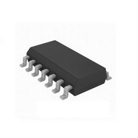
A hex inverter, also known as a hex NOT gate, is an integrated circuit (IC) that contains six independent inverter gates. Each inverter gate performs a logical NOT operation, which means it inverts the input signal. If the input is high (logical 1), the output will be low (logical 0), and vice versa.
The most common hex inverter ICs are the 7404 TTL (Transistor-Transistor Logic) and the 4069 CMOS (Complementary Metal-Oxide-Semiconductor) families. These ICs are widely used in digital circuits for their versatility and reliability.
Pinout and Package
Hex inverter ICs are available in various package types, such as DIP (Dual Inline Package), SOIC (Small Outline Integrated Circuit), and TSSOP (Thin Shrink Small Outline Package). The most common package is the 14-pin DIP, which has the following pinout:
| Pin | Function |
|---|---|
| 1 | 1A (Input 1) |
| 2 | 1Y (Output 1) |
| 3 | 2A (Input 2) |
| 4 | 2Y (Output 2) |
| 5 | 3A (Input 3) |
| 6 | 3Y (Output 3) |
| 7 | Ground |
| 8 | 4Y (Output 4) |
| 9 | 4A (Input 4) |
| 10 | 5Y (Output 5) |
| 11 | 5A (Input 5) |
| 12 | 6Y (Output 6) |
| 13 | 6A (Input 6) |
| 14 | VCC (Power Supply) |
How Does a Hex Inverter Work?
A hex inverter performs a simple logical operation called inversion or NOT. When the input is high (logical 1), the output will be low (logical 0), and when the input is low (logical 0), the output will be high (logical 1).
In a TTL hex inverter, such as the 7404, the inversion is achieved using a bipolar junction transistor (BJT) and resistors. The input signal is applied to the base of the transistor, which controls the collector-emitter current. When the input is high, the transistor is saturated, and the output is pulled low. When the input is low, the transistor is cut off, and the output is pulled high by the resistor connected to the power supply.
In a CMOS hex inverter, like the 4069, the inversion is performed using complementary MOSFETs (Metal-Oxide-Semiconductor Field-Effect Transistors). The input signal is applied to the gates of both the N-channel and P-channel MOSFETs. When the input is high, the N-channel MOSFET is on, and the P-channel MOSFET is off, pulling the output low. When the input is low, the P-channel MOSFET is on, and the N-channel MOSFET is off, pulling the output high.
Applications of Hex Inverters
Hex inverters find applications in various digital circuits, such as:
-
Logic gates: Hex inverters can be used to create other logic gates, like NAND, NOR, and XOR, by combining multiple inverters and using additional components like diodes or resistors.
-
Signal conditioning: Hex inverters can be used to clean up noisy or degraded signals by providing a sharp transition between logic levels.
-
Square wave generation: By connecting the output of an inverter to its input through a resistor and a capacitor, an astable multivibrator can be created, generating a square wave signal.
-
Buffer and driver circuits: Hex inverters can be used as buffers to isolate a sensitive circuit from a high-current load or to drive multiple loads without affecting the signal integrity.
-
Schmitt trigger: Some hex inverter ICs, like the 40106 CMOS Schmitt trigger, have built-in hysteresis, which helps to reduce the effects of noise and provide a clean output signal.

Designing with Hex Inverters
When designing circuits with hex inverters, there are several factors to consider:
Power Supply and Decoupling
Hex inverters require a stable power supply to function correctly. The power supply voltage (VCC) depends on the specific IC family:
- For TTL hex inverters (7404), VCC is typically 5V.
- For CMOS hex inverters (4069), VCC can range from 3V to 15V, depending on the specific part number.
To ensure proper operation and reduce noise, it is essential to include decoupling capacitors close to the VCC and ground pins of the IC. A typical value for the decoupling capacitor is 0.1µF ceramic capacitor.
Input and Output Characteristics
When interfacing hex inverters with other components or circuits, it is crucial to consider the input and output characteristics:
-
Input voltage levels: For TTL hex inverters, a voltage below 0.8V is considered a low input, and a voltage above 2V is considered a high input. For CMOS hex inverters, the input threshold voltage is typically around 50% of VCC.
-
Output current: Hex inverters have limited output current capability. For example, the 7404 TTL hex inverter can sink up to 16mA and source up to 400µA. If the load requires more current, an additional buffer or driver circuit may be necessary.
-
Propagation delay: The propagation delay is the time it takes for the output to change state after the input has changed. This delay varies depending on the IC family and the specific part number. For example, the 7404 has a typical propagation delay of 10ns, while the 4069 has a propagation delay of 60ns.
Noise Immunity and Unused Inputs
To improve noise immunity and prevent unwanted oscillations, it is recommended to connect unused inputs of a hex inverter to either VCC or ground, depending on the desired output state.
-
If an unused input is left floating, it may pick up noise and cause the output to oscillate or generate unwanted signals.
-
For TTL hex inverters, unused inputs should be connected to VCC through a pull-up resistor (typically 1kΩ to 10kΩ) to ensure a stable high output.
-
For CMOS hex inverters, unused inputs can be directly connected to VCC or ground, as they have built-in high-impedance inputs.
Comparing TTL and CMOS Hex Inverters
While both TTL and CMOS hex inverters perform the same basic function, they have some differences in terms of performance, power consumption, and compatibility.
| Characteristic | TTL (7404) | CMOS (4069) |
|---|---|---|
| Power Supply | 5V | 3V to 15V |
| Power Consumption | Higher | Lower |
| Speed | Faster | Slower |
| Noise Immunity | Lower | Higher |
| Output Current | Higher | Lower |
| Input Impedance | Lower | Higher |
In general, TTL hex inverters are faster and can drive higher output currents, making them suitable for high-speed applications or driving multiple loads. However, they consume more power and have lower noise immunity compared to CMOS hex inverters.
CMOS hex inverters, on the other hand, have lower power consumption, higher noise immunity, and a wider range of compatible power supply voltages. They are often used in low-power or battery-operated applications, as well as in environments with high electrical noise.
Troubleshooting and Common Issues
When working with hex inverters, some common issues may arise:
-
Incorrect power supply voltage: Ensure that the power supply voltage is within the specified range for the specific hex inverter IC. Applying an incorrect voltage can lead to malfunction or damage to the device.
-
Missing or incorrect decoupling capacitors: Always include decoupling capacitors close to the VCC and ground pins of the hex inverter to reduce noise and ensure stable operation. Verify that the capacitor values are correct and that they are properly connected.
-
Floating inputs: As mentioned earlier, leaving inputs floating can cause unwanted oscillations or noise. Make sure that all unused inputs are properly tied to VCC or ground, depending on the IC family and the desired output state.
-
Excessive load current: If the load connected to the output of the hex inverter draws more current than the IC can provide, the output voltage may drop, or the IC may be damaged. Use additional buffer or driver circuits if the load current exceeds the maximum ratings of the hex inverter.
-
Incorrect input voltage levels: Ensure that the input voltage levels are compatible with the specific hex inverter IC. Applying voltages outside the acceptable range can lead to incorrect operation or damage to the device.
FAQ
-
Q: Can a hex inverter be used as an amplifier?
A: No, a hex inverter is a digital logic device and cannot be used as an amplifier, which is an analog circuit that increases the amplitude of a signal. -
Q: How many gates are in a hex inverter?
A: A hex inverter contains six independent inverter gates. -
Q: Can hex inverters be cascaded to create a delay line?
A: Yes, by connecting the output of one inverter to the input of another, a delay line can be created. The total delay will be the sum of the propagation delays of each inverter in the chain. -
Q: Are hex inverters suitable for high-frequency applications?
A: The suitability of hex inverters for high-frequency applications depends on the specific IC family and part number. Some high-speed CMOS hex inverters, like the 74HC04 or 74AHC04, can operate at frequencies up to several hundred MHz. -
Q: Can a hex inverter be used to create a crystal oscillator?
A: Yes, a hex inverter can be used as the active component in a crystal oscillator circuit. By connecting a crystal and appropriate feedback components between the input and output of an inverter, a stable oscillator can be created.
Conclusion
Hex inverters are essential building blocks in digital electronics, providing a simple and efficient way to invert signals and create various logic functions. Understanding the characteristics, applications, and design considerations of hex inverters is crucial for anyone working with digital circuits.
By selecting the appropriate hex inverter IC family, properly interfacing with other components, and following best practices for power supply decoupling and input handling, designers can effectively incorporate hex inverters into their projects and create reliable, high-performance digital systems.

No responses yet