Introduction to 4-Layer PCB Benefits
4-layer PCBs offer many advantages over 2-layer PCBs for more complex and demanding electronics applications. The additional inner layers allow for more interconnect routing, better power delivery, and improved signal integrity compared to simpler 2-layer designs.
Some of the key benefits of using 4-layer PCBs include:
- Higher component density
- Improved EMI shielding
- Better power distribution
- Reduced crosstalk
- Controlled impedance
- Smaller board size
Let’s explore each of these 4-layer PCB benefits in more detail.
Higher Component Density with 4-Layer PCBs
One of the biggest advantages of 4-layer PCBs is the ability to accommodate a higher density of components on the board. The two additional inner layers provide more space for interconnect routing between components. This extra routing space is especially valuable for designs using fine-pitch surface mount devices with many pins that need to be routed.
With more available routing layers, the traces can be shorter, more direct, and occupy less area. Components can be placed closer together without worrying about routes crossing over each other. The PCB as a whole can shrink in size, allowing the electronics to fit in tighter spaces.
Some examples of high density electronics that utilize 4-layer PCBs include:
- Smartphones
- Smartwatches
- Wireless earbuds
- IoT devices
- Embedded controllers
In these types of products, the PCB space comes at a premium. Designers need to pack a lot of functionality into a very small footprint. Using 4-layer PCBs enables this level of miniaturization.
EMI Shielding with 4-Layer PCB Stack-ups
Electromagnetic interference (EMI) can be a major problem in sensitive electronic devices. Unwanted EMI can cause erratic operation, degrade signals, and even violate RF emissions regulations. 4-layer PCBs offer an effective way to mitigate EMI issues through proper stack-up design.
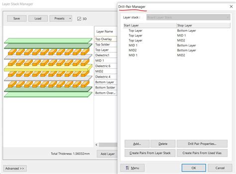
A typical 4-layer PCB stack-up has the following arrangement of copper layers:
| Layer | Purpose |
|---|---|
| Top | Signals + Components |
| Inner 1 | Ground Plane |
| Inner 2 | Power Plane |
| Bottom | Signals + Components |
The ground plane layer serves as an EMI shield between the top and bottom signal layers. Any noise coupled on to the signal traces gets shunted to ground. The large area of unbroken copper on the ground layer also prevents radiated emissions from the board itself.
Additionally, the power plane provides a low-impedance source of power distribution to the components. By minimizing the power path loops and centralizing power delivery, the overall EMI is reduced.
When done properly, a 4-layer PCB stack-up effectively creates a controlled EMI environment that is isolated from both internal and external interference sources. This EMI protection is critical for applications like:
- Wireless communication devices
- Medical electronics
- Automotive systems
- Industrial controls
- Military/aerospace gear

Power Distribution with 4-Layer PCBs
Clean, stable power delivery is essential for reliable circuit operation. As mentioned in the previous section, 4-layer PCBs usually dedicate one of the inner layers to power distribution. Having an entire layer for the power planes provides several power integrity benefits:
- Lower DC resistance
- Higher current carrying capacity
- Minimized voltage drops
- Decoupling capacitance
- Reduced EMI
By making the power planes as large and unbroken as possible, the DC resistance from the power source to the individual components is minimized. This improves voltage regulation and allows the PCB to supply higher currents.
The power plane also acts as a embedded decoupling capacitor formed by the overlapping area with the adjacent ground plane. This helps filter high-frequency noise on the power rails.
Compared to using thin traces on a 2-layer board, the use of full power planes on a 4-layer board significantly improves the power delivery network (PDN) performance. This is especially important for power-hungry, noise-sensitive components like:
- FPGAs
- Microprocessors
- RF transceivers
- ADCs/DACs
- Sensors
- LEDs
Reduced Crosstalk with 4-Layer PCBs
Crosstalk happens when signals on adjacent traces capacitively couple and interfere with each other. The coupling induces voltage spikes that can cause false triggering, corrupt data, and other malfunctions. Crosstalk gets worse with long parallel trace runs, fast signal rise/fall times, and tight spacing.
4-layer PCBs provide several ways to combat crosstalk:
- Shorter traces
- Increased spacing
- Orthogonal routing
- Shielding with planes
As covered in earlier sections, 4-layer PCBs accommodate higher component density and have more routing space. This allows signal traces to be shorter and spaced further apart, minimizing the coupling area.
For long bus runs, 4-layer PCBs have enough room to route adjacent layers perpendicular to each other. Traces on the top can run horizontally while traces on the bottom run vertically. This “X-Y” routing technique eliminates broadside coupling.
The power and ground planes also shield the top and bottom layers from each other. Any stray coupling gets absorbed by the low-impedance planes in between.
Reducing crosstalk is important for designs with:
- High-speed digital interfaces
- Analog/RF sections
- Mixed-signal circuitry
- Impedance controlled traces
- Noisy environments
Controlled Impedance with 4-Layer PCBs
Many high-speed interfaces like USB, Ethernet, PCIe, and DDR have strict impedance requirements for the signal traces. If the traces deviate from the target impedance, signal integrity issues arise from reflections, attenuation, and crosstalk.
4-layer PCBs allow for very precise control of trace impedances. By adjusting the trace width and the spacing to the reference plane(s), the impedance can be fine-tuned to meet specs. The continuous power and ground planes establish consistent reference layers for the impedance calculations.
The impedance targets are determined by the dielectric properties of the PCB substrate, the copper weight, and the overall stack-up thicknesses. With a 4-layer stack-up, the impedances can be approximated using the following formulas:
For microstrip (outer layers):
Z0 = 87 / (√εr + 1.41) * ln(5.98 * h / (0.8 * w + t))
For stripline (inner layers):
Z0 = 60 / √εr * ln(4 * h / (0.67 * π * (0.8 * w + t)))
Where:
– Z0 = characteristic impedance (Ω)
– εr = dielectric constant of substrate
– h = dielectric thickness (m)
– w = trace width (m)
– t = trace thickness (m)
By modeling the stack-up in PCB layout tools and using field solvers, designers can precisely calculate the geometry needed to achieve the target impedances. This level of impedance control is very difficult with 2-layer PCBs.
Compact Form Factors with 4-Layer PCBs
All of the 4-layer PCB benefits covered so far ultimately allow the Electronics to shrink in size. The higher component density, better EMI control, centralized power delivery, reduced crosstalk, and precise impedance control mean the circuitry can be routed in less area.
This is extremely valuable for space-constrained applications like:
- Wearables
- Portable instruments
- Miniature sensors
- Implantable medical devices
- Smartphones/tablets
- Drones
In many cases, the PCB is the largest contributor to the overall size of the electronics. By leveraging the efficiency of a 4-layer design, products can slim down their form factors significantly.
4-Layer vs 2-Layer Cost Comparison
Despite all the benefits, 4-layer PCBs do have a notable drawback – increased cost. Compared to 2-layer boards, 4-layer boards require additional fabrication steps, more material, and greater manufacturing precision. This raises the cost-per-unit, especially in small to medium volumes.
However, the cost difference may not be as dramatic as you would expect. Let’s consider some real numbers from a typical PCB manufacturer:
| Layers | Dimensions | Quantity | Lead Time | Price |
|---|---|---|---|---|
| 2 | 100 x 100 mm | 5 | 5 days | $88 |
| 4 | 100 x 100 mm | 5 | 6 days | $166 |
In this case, the 4-layer version is about 1.9x the cost of the 2-layer version for the same size and quantity. While this is a significant increase, the actual dollar amount is fairly reasonable – only $78 more for a set of 5 boards. Considering the performance and reliability gains of the 4-layer design, this premium may be well worth it for many applications.
As the quantities increase, the cost multiplier of a 4-layer board over a 2-layer shrinks:
| Layers | Dimensions | Quantity | Lead Time | Price |
|---|---|---|---|---|
| 2 | 100 x 100 mm | 1000 | 8 days | $1,475 |
| 4 | 100 x 100 mm | 1000 | 10 days | $2,242 |
At 1000 pcs, the 4-layer boards are only about 1.5x the cost of the 2-layer. Again, for an annual production run, this ∼$800 difference may be negligible compared to the improved performance and reliability.
FAQ
Q1: Are 4-layer PCBs always better than 2-layer?
Not necessarily. For simple designs with low component count, relaxed routing requirements, and non-critical signals, a 2-layer board is usually adequate and more cost-effective. 4-layer boards excel in complex designs that have challenging signal integrity, power delivery, or EMI shielding demands.
Q2: Do 4-layer PCBs require special design rules?
Yes, 4-layer PCBs have additional considerations beyond 2-layer design rules. The stack-up arrangement, trace widths/spacing, via spans, and plane cuts need to be specified. Typically the fabricator will provide a 4-layer design rules document that lists all the specific parameters to follow.
Q3: Can 4-layer PCBs be mixed with 2-layer?
Sometimes designs use 4-layer for the main high-speed digital section and 2-layer for simpler analog/power sections to save cost. The 2-layer and 4-layer “modules” are then connected together with board-to-board headers or flex cables. However, this partitioned approach is only practical for very specific applications.
Q4: Are there even higher layer count PCBs beyond 4-layer?
Yes, PCBs can have 6, 8, 10, 12 or even more layers in very demanding applications. Backplanes, FPGAs, supercomputer boards, and telecom switches are some examples of designs that use 8 layers or more. In general, higher layer counts are used to accommodate very large, complex chips with thousands of pins.
Q5: What industries commonly use 4-layer PCBs?
4-layer PCBs see wide adoption in industries with electronics that have:
- High speed digital interfaces
- Wireless/RF communication
- Low power consumption requirements
- Compact form factors
- Harsh operating environments
- Safety-critical functions
Some of the biggest consumers of 4-layer PCBs include consumer electronics, automotive, aerospace, medical devices, industrial automation, and telecom infrastructure.
Conclusion
In summary, 4-layer PCBs provide compelling benefits over traditional 2-layer PCBs, including:
- Higher component density
- Improved EMI shielding
- Better power distribution
- Reduced crosstalk
- Controlled impedance
- Smaller form factors
For modern electronics with demanding performance, signal integrity, and reliability requirements, 4-layer PCBs have become the go-to solution. While they do come at an increased cost, the advantages can easily outweigh the added expense.
As PCB manufacturing continues to advance, we can expect 4-layer boards to become even more capable and cost-effective over time. Designers who embrace the benefits of 4-layer PCBs will be well-positioned to create cutting-edge electronics that meet the needs of today and tomorrow.

No responses yet