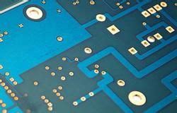
Introduction to Multilayer PCB Fabrication
Printed Circuit Boards (PCBs) have revolutionized the electronics industry by providing a reliable and efficient means of connecting electronic components. As technology advances and devices become more complex, the demand for high-density interconnects and compact designs has led to the development of multilayer PCBs. Multilayer PCB fabrication involves the process of layering and bonding multiple single-layer PCBs to create a single, cohesive board with enhanced functionality and performance.
In this article, we will delve into the intricacies of multilayer PCB fabrication, focusing on the critical steps of lay-up and bonding. We will explore the various techniques, materials, and considerations involved in creating a high-quality multilayer PCB that meets the stringent requirements of modern electronic devices.
Understanding the Basics of Multilayer PCBs
Before we dive into the lay-up and bonding process, let’s first understand the fundamentals of multilayer PCBs.
What is a Multilayer PCB?
A multilayer PCB is a printed circuit board that consists of three or more conductive layers laminated together with insulating material between each layer. These layers are interconnected through plated through-holes (PTHs) or via holes, allowing for complex routing and increased component density.
Advantages of Multilayer PCBs
Multilayer PCBs offer several advantages over single-layer or double-layer PCBs:
- Increased component density: Multilayer PCBs allow for more components to be placed on a smaller board size, enabling compact and space-efficient designs.
- Enhanced signal integrity: The use of dedicated power and ground planes in multilayer PCBs helps reduce electromagnetic interference (EMI) and improves signal integrity.
- Improved thermal management: The increased number of layers in a multilayer PCB provides better heat dissipation, allowing for more efficient cooling of components.
- Reduced crosstalk: The separation of signal layers by ground or power planes minimizes crosstalk between adjacent traces.
Common Multilayer PCB Stackups
Multilayer PCBs can have various stackups depending on the number of layers and the specific requirements of the application. Some common multilayer PCB stackups include:
| Layers | Stackup |
|---|---|
| 4 | Signal – Ground – Power – Signal |
| 6 | Signal – Ground – Signal – Signal – Ground – Signal |
| 8 | Signal – Ground – Signal – Power – Signal – Ground – Signal – Signal |
| 10 | Signal – Ground – Signal – Power – Ground – Power – Signal – Ground – Signal – Signal |
The choice of stackup depends on factors such as the required signal integrity, power distribution, and overall board thickness.

The Lay-up Process in Multilayer PCB Fabrication
The lay-up process is a critical step in multilayer PCB fabrication, where the individual layers are stacked and aligned before bonding. Let’s explore the various aspects of the lay-up process.
Preparing the Inner Layers
The first step in the lay-up process is to prepare the inner layers of the multilayer PCB. These layers are typically double-sided copper-clad laminates (CCLs) that have been patterned and etched to create the desired Circuit Traces and pads.
The inner layers undergo the following steps:
- Cleaning: The inner layers are thoroughly cleaned to remove any contaminants or residues that may affect the bonding process.
- Oxide treatment: The copper surfaces of the inner layers are treated with an oxide to improve adhesion during the bonding process.
- Inspection: The inner layers are inspected for any defects or irregularities that may impact the final PCB Quality.
Preparing the Prepreg and Core Materials
In addition to the inner layers, the lay-up process also involves the preparation of the prepreg and core materials.
Prepreg (pre-impregnated) is a glass fabric that is pre-impregnated with a partially cured resin. It acts as an insulating layer between the conductive layers of the PCB. The prepreg is cut to the required size and shape, and any necessary openings for vias or component holes are punched or drilled.
Core materials, such as FR-4, are used as the base substrate for the multilayer PCB. They provide mechanical stability and insulation between the outer layers of the board.
Stacking and Aligning the Layers
Once the inner layers, prepreg, and core materials are prepared, they are carefully stacked and aligned to form the multilayer PCB stackup.
The stacking process follows a specific order, alternating between the inner layers, prepreg, and core materials. The alignment is critical to ensure that the vias and component holes line up accurately across all layers.
Alignment pins or fixtures are often used to maintain the precise positioning of the layers during the stacking process. Optical alignment systems may also be employed for high-precision alignment requirements.
Preparing for Bonding
After the layers are stacked and aligned, they are prepared for the bonding process. This typically involves the following steps:
- Lamination press preparation: The stacked layers are placed in a lamination press, which applies heat and pressure to bond the layers together.
- Vacuum bagging: The stacked layers may be vacuum bagged to remove any air pockets and ensure even pressure distribution during bonding.
- Lamination parameter setup: The lamination press parameters, such as temperature, pressure, and duration, are set according to the specific requirements of the PCB material and stackup.

The Bonding Process in Multilayer PCB Fabrication
The bonding process is the final step in creating a cohesive multilayer PCB. It involves the application of heat and pressure to fuse the layers together and cure the prepreg resin.
Lamination Press Operation
The lamination press is a critical equipment in the bonding process. It applies a combination of heat and pressure to the stacked layers, causing the prepreg resin to flow and cure, effectively bonding the layers together.
The lamination press typically consists of heated platens that compress the PCB stackup between them. The specific temperature, pressure, and duration of the lamination process depend on the type of prepreg and the thickness of the PCB.
Common lamination press parameters include:
| Parameter | Typical Range |
|---|---|
| Temperature | 180°C – 200°C |
| Pressure | 200 – 400 psi |
| Duration | 60 – 120 minutes |
Precise control of these parameters is essential to ensure a strong and reliable bond between the layers.
Cooling and Stabilization
After the lamination process, the bonded multilayer PCB undergoes a cooling and stabilization period. This allows the PCB to gradually return to room temperature and the resin to fully cure and stabilize.
Proper cooling is important to prevent warping or delamination of the PCB due to thermal stress. The cooling rate is typically controlled to ensure a gradual and even temperature reduction across the board.
Inspection and Quality Control
Once the bonded multilayer PCB has cooled and stabilized, it undergoes a thorough inspection and quality control process. This includes:
- Visual inspection: The PCB is visually inspected for any signs of delamination, warping, or other defects.
- Electrical testing: Continuity and isolation tests are performed to verify the integrity of the electrical connections and the absence of short circuits.
- Microsectioning: In some cases, a small section of the PCB may be cut and analyzed under a microscope to assess the quality of the bonding and the integrity of the vias and plated through-holes.
Any boards that fail the inspection and quality control process are rejected and may be reworked or scrapped depending on the nature and severity of the defects.

Challenges and Considerations in Multilayer PCB Fabrication
While multilayer PCB fabrication offers numerous benefits, it also presents several challenges and considerations that must be addressed to ensure a successful and reliable end product.
Material Selection
The choice of materials for the inner layers, prepreg, and core of a multilayer PCB is crucial. Factors to consider include:
- Dielectric constant: The dielectric constant of the insulating materials affects the signal propagation and impedance of the PCB.
- Glass transition temperature (Tg): The Tg of the materials determines their thermal stability and resistance to deformation during the lamination process.
- Coefficient of thermal expansion (CTE): Mismatches in CTE between different materials can lead to thermal stress and potential reliability issues.
Careful selection of materials with compatible properties is essential to ensure the longevity and performance of the multilayer PCB.
Signal Integrity and Crosstalk
As the number of layers and the density of components increase in a multilayer PCB, signal integrity and crosstalk become significant concerns.
To mitigate these issues, designers must consider:
- Proper stackup design: The arrangement of signal, ground, and power layers in the stackup can help minimize crosstalk and improve signal integrity.
- Impedance control: Maintaining consistent impedance throughout the signal paths is crucial for high-speed designs.
- Via optimization: The placement, size, and type of vias can impact signal integrity and must be carefully considered.
Simulation tools and analysis techniques, such as signal integrity analysis and crosstalk simulation, can help designers optimize the PCB layout for improved signal integrity.
Thermal Management
Multilayer PCBs with high component density generate significant amounts of heat, which must be effectively dissipated to ensure reliable operation.
Thermal management strategies for multilayer PCBs include:
- Thermal vias: The use of thermal vias to transfer heat from inner layers to the outer layers and heatsinks.
- Copper pours: Incorporating copper pours on unused areas of the PCB can help distribute heat more evenly.
- Thermal interface materials: The use of thermal interface materials between the PCB and heatsinks can enhance heat transfer.
Proper thermal management is essential to prevent overheating, which can lead to component failure and reduced PCB lifespan.
Manufacturing Complexity and Cost
As the number of layers and the complexity of the PCB increase, so does the manufacturing complexity and cost.
Factors that contribute to the increased complexity and cost include:
- Increased processing steps: Each additional layer in the PCB requires additional processing steps, such as etching, lamination, and drilling.
- Higher material costs: The use of specialized materials, such as high-performance laminates or low-loss prepregs, can increase the overall material cost.
- Tighter tolerances: Multilayer PCBs often require tighter manufacturing tolerances, which can increase the cost and lead time.
Designers must balance the performance requirements of the PCB with the manufacturing complexity and cost to ensure a cost-effective and feasible solution.
FAQ
-
What is the purpose of the lay-up process in multilayer PCB fabrication?
The lay-up process is a critical step in multilayer PCB fabrication where the individual layers, including the inner layers, prepreg, and core materials, are stacked and aligned before bonding. This process ensures the precise positioning and alignment of the layers to form the desired multilayer PCB stackup. -
What is the role of prepreg in multilayer PCB fabrication?
Prepreg (pre-impregnated) is a glass fabric that is pre-impregnated with a partially cured resin. It acts as an insulating layer between the conductive layers of the PCB. During the bonding process, the prepreg resin flows and cures, bonding the layers together to form a cohesive multilayer PCB. -
What are the key parameters controlled during the lamination process?
The key parameters controlled during the lamination process are temperature, pressure, and duration. Typical ranges for these parameters include a temperature of 180°C – 200°C, pressure of 200 – 400 psi, and duration of 60 – 120 minutes. Precise control of these parameters is essential to ensure a strong and reliable bond between the layers. -
Why is thermal management important in multilayer PCB fabrication?
Multilayer PCBs with high component density generate significant amounts of heat, which must be effectively dissipated to ensure reliable operation. Proper thermal management strategies, such as the use of thermal vias, copper pours, and thermal interface materials, help prevent overheating, which can lead to component failure and reduced PCB lifespan. -
How does the number of layers affect the manufacturing complexity and cost of a multilayer PCB?
As the number of layers in a multilayer PCB increases, so does the manufacturing complexity and cost. Each additional layer requires additional processing steps, such as etching, lamination, and drilling. Higher layer counts may also necessitate the use of specialized materials and tighter manufacturing tolerances, further increasing the cost and lead time of the PCB.
Conclusion
Multilayer PCB fabrication is a complex process that involves the careful layering and bonding of multiple conductive and insulating layers to create a high-density, high-performance circuit board. The lay-up and bonding processes are critical steps in ensuring the precise alignment and reliable bonding of the layers.
Designers and manufacturers must consider various factors, such as material selection, signal integrity, thermal management, and manufacturing complexity, to create a multilayer PCB that meets the demands of modern electronic devices.
By understanding the intricacies of multilayer PCB fabrication and following best practices in design and manufacturing, engineers can unleash the full potential of this powerful technology to create innovative and reliable electronic products.
No responses yet