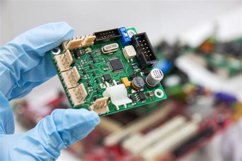
What is PCB Assembly?
PCB assembly is the process of attaching electronic components to a printed circuit board (PCB) to create a functional electronic assembly. The PCB serves as the foundation for the assembly, providing the conductive pathways that interconnect the various components.
PCB assembly involves several key steps:
- Solder Paste Application
- Component Placement
- Reflow Soldering
- Inspection and Testing
- Final Assembly
Let’s explore each of these steps in more detail.
Solder Paste Application
The first step in PCB assembly is applying solder paste to the PCB. Solder paste is a mixture of tiny solder spheres suspended in flux. It is applied to the PCB’s surface mount pads using a solder paste stencil and squeegee.
The stencil is a thin metal sheet with apertures that match the PCB’s solder pads. It is aligned precisely with the PCB and held in place. Then solder paste is deposited over the stencil and a squeegee is used to spread the paste evenly, forcing it through the apertures and onto the pads.
Solder paste is a key material that affects the quality of the final solder joints. Some important solder paste properties include:
| Property | Description |
|---|---|
| Alloy Type | The metals that make up the solder, typically tin, lead, silver, copper |
| Particle Size | The diameter of the solder spheres, which affects printability and reflow |
| Flux Type | Rosin, no-clean, or water-soluble flux that removes oxides during reflow |
| Viscosity | Paste’s resistance to flow, which affects stencil printing and slump |
Precise solder paste deposition is crucial for achieving reliable solder joints. Too little paste can result in open circuits, while too much can cause short circuits.
Component Placement
After solder paste printing, the next step is placing components onto the PCB. Surface mount components are placed with pick-and-place machines. These automated systems use vacuum nozzles to pick up components from feeders and accurately place them onto their respective solder paste deposits.
Placement machines have several key characteristics:
| Specification | Description |
|---|---|
| Accuracy | Placement precision, typically ±50 μm or better |
| Speed | Components placed per hour (CPH), ranging from thousands to over 100,000 |
| Component Range | Smallest and largest component sizes the machine can handle |
| Feeder Capacity | Number of component reels or trays the machine supports |
| Vision System | Cameras for fiducial alignment and component inspection |
Placement accuracy is critical to ensure components are properly aligned and centered on their pads. Misaligned components can result in poor solder joints or even falls during reflow.
Some PCB designs may also have through-hole components that are inserted manually or with selective soldering after surface mount placement.
Reflow Soldering
After components are placed, the entire PCB assembly is run through a reflow oven to permanently solder the components. The reflow oven heats the assembly in a controlled manner, following a specific reflow profile that is tailored to the solder paste and PCB characteristics.
A typical reflow profile consists of four stages:
- Preheat: The assembly is gradually heated to evaporate solvents and activate the flux.
- Thermal Soak: Temperature is held steady to equalize across the assembly.
- Reflow: Temperature is peaked above the solder’s melting point, causing the paste to reflow and form solder joints.
- Cooling: Assembly is cooled to solidify the solder joints.
Here is an example of a lead-free reflow profile:
| Stage | Temperature | Duration |
|---|---|---|
| Preheat | 25°C to 150°C | 60-90 seconds |
| Thermal Soak | 150°C to 200°C | 60-120 seconds |
| Reflow | 235°C to 250°C peak | 30-90 seconds above 217°C |
| Cooling | Peak to 100°C | 60-120 seconds |
The specific parameters of the reflow profile depend on factors such as the PCB’s thermal mass, component density, and solder paste composition. An optimized reflow profile will fully melt the solder and form reliable joints without damaging components through excessive heat exposure.
Inspection and Testing
After reflow soldering, the PCB assembly is inspected and tested to verify its quality and functionality. Several methods are commonly used:
-
Visual Inspection: Trained operators or automated optical inspection (AOI) systems check for visible defects such as misaligned components, solder bridges, or missing solder joints.
-
X-Ray Inspection: Transmits X-rays through the assembly to image solder joints hidden under components like ball grid arrays (BGAs). Used to detect voids, shorts, or opens.
-
In-Circuit Test (ICT): Fixture-based test that probes test points on the PCB to verify component values, circuit continuity, and basic functionality.
-
Functional Test: Applies power to the assembly and verifies end-to-end functionality, often with automated test equipment (ATE) and test software.
The choice of inspection and test methods depends on the PCB’s complexity, reliability requirements, and production volume. Generally, a combination of methods is used to maximize defect coverage.
Some key metrics used to quantify PCB assembly quality include:
| Metric | Description | Formula |
|---|---|---|
| First Pass Yield (FPY) | Percentage of assemblies that pass all tests on the first attempt | FPY = (Units Passed ÷ Units Tested) × 100 |
| Defects per Million Opportunities (DPMO) | Number of defects found per million solder joints | DPMO = (Defects ÷ Opportunities) × 1,000,000 |
| Rolled Throughput Yield (RTY) | Probability that an assembly will pass through the entire process defect-free | RTY = FPY1 × FPY2 × … × FPYn |
Higher FPY and RTY values and lower DPMO values indicate a more capable and controlled PCB assembly process.
Final Assembly
After PCB assembly and testing are complete, the PCB often undergoes final assembly steps before it is ready for use in a end product. This can include:
-
Mechanical Assembly: The PCB is installed into an enclosure or chassis along with other mechanical components.
-
Wiring and Cabling: Power and signal cables are connected to the PCB as needed to interface with other system components.
-
Programming and Calibration: Firmware is loaded onto the PCB’s processors and the assembly is calibrated or configured for end use.
-
Packaging and Shipping: The final product is packaged to protect it from damage and shipped to the end customer.
The specifics of the final assembly process vary widely depending on the type of product being manufactured.
Types of PCB Assembly
There are three main types of PCB assembly, each with its own characteristics and use cases.
Surface Mount Technology (SMT) Assembly
SMT assembly is the most common PCB assembly method today. In this process, components are mounted directly onto the surface of the PCB.
SMT components have small metal leads or terminals that are soldered to pads on the PCB’s surface. Common SMT package types include:
- Chip components: Resistors, capacitors, inductors
- Flat pack ICs: Quad Flat Packs (QFP), Small Outline ICs (SOIC)
- Leadless packages: Quad Flat No-leads (QFN), Land Grid Arrays (LGA)
- Ball Grid Arrays (BGA): Arrays of solder balls underneath the component
SMT allows for much smaller components and higher density PCB designs compared to through-hole assembly. It also enables components to be mounted on both sides of the board. Nearly all modern high-volume electronics use SMT assembly.
However, SMT requires specialized equipment and processes for solder paste printing, component placement, and reflow soldering. Defects can be harder to detect and rework compared to through-hole.
Through-Hole Technology (THT) Assembly
THT assembly is a traditional PCB assembly method where component leads are inserted through drilled holes in the PCB and soldered to pads on the opposite side.
THT components include:
- Axial components: Resistors, capacitors with wire leads
- Radial components: Capacitors, LEDs with leads on one side
- DIP ICs: Dual In-Line Packages with two rows of leads
THT provides strong mechanical bonds for components subjected to high stress. It is often used for connectors, large power components, or parts not available in SMT packages.
However, THT has largely been replaced by SMT in most applications due to its lower density, higher cost, and manual assembly requirements. Most THT assemblies are now done with selective soldering machines rather than manual soldering.
Mixed Technology Assembly
Many PCB designs use a mix of SMT and THT components to leverage the advantages of both. A typical mixed assembly process flow is:
- SMT solder paste printing
- SMT component placement
- Reflow soldering of SMT components
- THT component insertion
- Wave or selective soldering of THT components
Mixed assembly allows designers to use THT connectors and large components alongside SMT chips. However, it adds process steps and requires careful planning to avoid issues like solder bridging between SMT and THT components.

PCB Assembly Services
PCB assembly can be done in-house by a company or outsourced to a specialized assembly provider. Each option has its own trade-offs.
In-House Assembly
In-house PCB assembly gives a company full control over the assembly process and quality. It can provide faster turnaround times and greater flexibility for prototypes and low-volume production.
However, in-house assembly requires significant capital investment in equipment, facilities, and staffing. It also requires ongoing process development and maintenance to keep up with changing technologies and quality requirements.
In-house assembly makes the most sense for companies with high volumes, unique process needs, or proprietary designs they want to protect. Many large electronics OEMs maintain some in-house assembly capability.
Outsourced Assembly
Outsourcing PCB assembly to a contract manufacturer (CM) or Electronics Manufacturing Services (EMS) provider is a popular option for many companies. Outsourcing provides access to specialized expertise, equipment, and economies of scale.
PCB assembly services can include:
- Turnkey assembly: The provider sources components and handles the entire assembly process.
- Partial turnkey: The customer provides some components or materials and the provider handles the rest.
- Consignment: The customer provides all components and the provider does the assembly labor.
Outsourcing allows companies to focus on their core competencies of design and marketing while leveraging the manufacturing capabilities of their assembly partners. It reduces capital requirements and provides flexibility to scale production up or down as needed.
However, outsourcing also involves trade-offs in control, communication, and intellectual property protection. It requires careful selection and management of assembly partners to ensure quality, reliability, and continuity of supply.

Choosing a PCB Assembly Partner
If outsourcing PCB assembly, selecting the right partner is critical to the success of the project. Key factors to consider include:
-
Technical Capabilities: Does the provider have experience with the needed technologies, materials, and processes? Can they handle the complexity and volume of the project?
-
Quality Systems: Does the provider have robust quality control and inspection processes in place? Do they have relevant quality certifications like ISO 9001, AS9100, or IPC-A-610?
-
Capacity and Lead Times: Can the provider scale to meet volume needs and deliver on time? Do they have multiple facilities for risk mitigation?
-
Engineering Support: Does the provider offer design for manufacturability (DFM) feedback and support? Can they help optimize the design for cost and reliability?
-
Supply Chain: Does the provider have a strong supply chain for sourcing components? Can they manage obsolescence and counterfeit risk?
-
Communication and Reporting: Does the provider communicate proactively and provide regular status updates? Do they offer robust reporting and traceability?
-
Cost and Value: Is the provider cost-competitive for the services offered? Do they provide value-added services that can save time and money?
Evaluating potential assembly partners across these dimensions through site visits, audits, and reference checks can help ensure a successful outsourcing relationship.

Future Trends in PCB Assembly
PCB assembly technology continues to evolve to meet the needs of advancing electronics. Some key trends shaping the future of PCB assembly include:
-
Miniaturization: As devices get smaller and more complex, PCBs need to pack more functionality into less space. This drives the need for finer pitches, thinner materials, and high-density interconnects.
-
Advanced Packaging: Newer component packaging technologies like wafer-level packaging (WLP), package-on-package (PoP), and embedded die are blurring the lines between ICs and PCBs.
-
Flexible and Stretchable Electronics: Flexible printed circuits (FPCs) and stretchable electronics are enabling new form factors for wearables, medical devices, and IoT sensors. These require new materials and assembly processes.
-
Additive Manufacturing: 3D printing technologies like inkjet and aerosol jet printing are being used to directly print conductors, resistors, and other features onto PCBs. This can enable rapid prototyping, customization, and new design possibilities.
-
Automation and Industry 4.0: Smart factory technologies like machine vision, robots, and big data analytics are being applied to PCB assembly to improve quality, traceability, and efficiency. This can enable lights-out manufacturing and faster New Product Introductions.
Staying on top of these technology trends is critical for electronics companies and their PCB assembly partners to stay competitive in a fast-moving industry.
Frequently Asked Questions
What is the difference between PCB fabrication and PCB assembly?
PCB fabrication is the process of manufacturing the bare printed circuit board, including etching the copper traces, drilling holes, and applying solder mask and silkscreen. PCB assembly is the process of attaching components to the fabricated PCB to create a functional circuit assembly.
What is the difference between surface mount and through-hole assembly?
Surface mount assembly mounts components directly onto the surface of the PCB, while through-hole assembly inserts component leads through holes in the board and solders them to pads on the opposite side. Surface mount allows for smaller components and higher density, while through-hole provides stronger mechanical bonds.
What is a solder paste stencil and why is it used?
A solder paste stencil is a thin metal sheet with apertures that match the PCB’s solder pads. It is used to apply solder paste to the pads in a precise and repeatable manner. The stencil ensures the right amount of paste is deposited in the right locations for reliable component attachment.
What is reflow soldering and how does it work?
Reflow soldering is a process that uses heat to melt and flow solder paste to permanently attach components to a PCB. The PCB assembly is run through a reflow oven which heats it in a controlled profile to activate the flux, melt the solder, and form solder joints. The solder then cools and solidifies to create the electrical and mechanical bonds.
How do I choose a PCB assembly partner?
Choosing a PCB assembly partner requires evaluating their technical capabilities, quality systems, capacity, engineering support, supply chain, communication, and cost. It’s important to select a partner that has experience with your specific technologies and requirements and can scale to meet your needs. Conducting site visits, audits, and reference checks can help ensure a good fit.
No responses yet