Introduction to PCB Stackup
PCB stackup refers to the arrangement of copper layers and insulating materials that make up a printed circuit board (PCB). It is a critical aspect of PCB design, as it determines the electrical characteristics, signal integrity, and manufacturability of the board. In this article, we will focus on the basic stackup of a 16-layer PCB board, exploring its structure, benefits, and design considerations.
Understanding the 16 Layer PCB Stackup
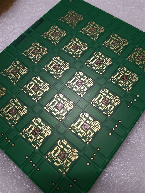
A 16-layer PCB is a complex and high-density board that is commonly used in advanced electronic applications, such as telecommunications, aerospace, and military systems. The basic stackup of a 16-layer PCB consists of the following layers:
| Layer | Description |
|---|---|
| Top Layer | Signal layer, component placement |
| Ground Layer | Ground plane |
| Signal Layer 1 | Signal routing |
| Signal Layer 2 | Signal routing |
| Ground Layer | Ground plane |
| Signal Layer 3 | Signal routing |
| Signal Layer 4 | Signal routing |
| Power Layer | Power plane |
| Signal Layer 5 | Signal routing |
| Signal Layer 6 | Signal routing |
| Ground Layer | Ground plane |
| Signal Layer 7 | Signal routing |
| Signal Layer 8 | Signal routing |
| Ground Layer | Ground plane |
| Signal Layer 9 | Signal routing |
| Bottom Layer | Signal layer, component placement |
The stackup alternates between signal layers and ground/power planes, providing a stable and noise-free environment for signal transmission. The ground planes help to reduce electromagnetic interference (EMI) and crosstalk between signal layers, while the power planes distribute power evenly across the board.
Signal Layers
The signal layers are responsible for routing the electrical signals between components on the PCB. In a 16-layer board, there are typically 10 signal layers, which are divided into pairs. Each pair is separated by a ground or power plane to minimize crosstalk and interference.
When designing the signal layers, it is essential to consider the following factors:
- Trace width and spacing: The width and spacing of the traces should be optimized to achieve the desired impedance and minimize signal reflections.
- Via placement: Vias should be strategically placed to minimize the length of signal paths and reduce the number of layer transitions.
- Signal integrity: High-speed signals should be routed carefully to maintain signal integrity and avoid issues such as ringing, overshoot, and undershoot.
Ground and Power Planes
The ground and power planes serve several important functions in a 16-layer PCB stackup:
- EMI reduction: The ground planes act as shields between signal layers, reducing electromagnetic interference and crosstalk.
- Power distribution: The power planes provide a low-impedance path for distributing power to components on the board.
- Heat dissipation: The ground and power planes help to spread heat evenly across the board, improving thermal management.
When designing the ground and power planes, it is important to ensure that they are properly connected to the signal layers through vias and that they have sufficient copper coverage to maintain a low-impedance path.

Benefits of a 16 Layer PCB Stackup
Using a 16-layer PCB stackup offers several advantages over boards with fewer layers:
- Increased routing density: With 10 signal layers, a 16-layer board provides ample space for routing complex circuits and high-density designs.
- Improved signal integrity: The alternating arrangement of signal layers and ground/power planes helps to maintain signal integrity and minimize noise and interference.
- Better power distribution: The dedicated power planes ensure that power is distributed evenly across the board, reducing voltage drops and improving overall system performance.
- Enhanced thermal management: The ground and power planes help to dissipate heat more efficiently, reducing thermal stress on components and improving reliability.

Design Considerations for 16 Layer PCB Stackup
When designing a 16-layer PCB stackup, there are several key considerations to keep in mind:
- Material selection: Choose high-quality materials with consistent dielectric properties to ensure reliable performance and manufacturability.
- Impedance control: Carefully design the trace widths and spacings to achieve the desired impedance and minimize signal reflections.
- Via optimization: Optimize the size and placement of vias to minimize the length of signal paths and reduce the number of layer transitions.
- Differential signaling: Use differential signaling when routing high-speed signals to reduce noise and improve signal integrity.
- Signal integrity analysis: Conduct thorough signal integrity analysis to ensure that signals meet timing and quality requirements.

Challenges of 16 Layer PCB Design
Designing a 16-layer PCB presents several challenges that must be addressed to ensure a successful outcome:
- Increased complexity: With so many layers and components, a 16-layer board is inherently more complex than boards with fewer layers, requiring more advanced design tools and expertise.
- Manufacturing limitations: Not all PCB manufacturers have the capability to produce 16-layer boards, and those that do may have specific requirements for materials, trace widths, and spacings.
- Cost: Due to the complexity and specialized manufacturing processes involved, 16-layer PCBs are typically more expensive than boards with fewer layers.
- Design time: Designing a 16-layer board requires more time and effort than simpler boards, as each layer must be carefully planned and optimized for performance and manufacturability.
Frequently Asked Questions (FAQ)
1. What is the typical thickness of a 16-layer PCB?
A 16-layer PCB can vary in thickness depending on the specific application and design requirements. However, a typical thickness for a 16-layer board is around 0.093 inches (2.36 mm) to 0.125 inches (3.18 mm).
2. Can a 16-layer PCB be manufactured using standard FR-4 material?
Yes, a 16-layer PCB can be manufactured using standard FR-4 material. However, for high-speed or high-frequency applications, it may be necessary to use higher-performance materials such as Rogers or Isola to achieve the desired electrical characteristics.
3. How long does it take to design and manufacture a 16-layer PCB?
The design and manufacturing time for a 16-layer PCB can vary depending on the complexity of the design and the availability of materials and manufacturing resources. Typically, the design process can take several weeks, while manufacturing can take an additional 2-3 weeks.
4. Are there any special testing requirements for 16-layer PCBs?
Yes, 16-layer PCBs require specialized testing to ensure that they meet performance and reliability requirements. This may include high-speed signal integrity testing, thermal analysis, and advanced visual inspection techniques.
5. Can a 16-layer PCB be reworked or repaired?
Reworking or repairing a 16-layer PCB can be challenging due to the complexity of the board and the difficulty in accessing inner layers. In many cases, it may be more cost-effective to replace the entire board rather than attempting a repair.
Conclusion
The basic stackup of a 16-layer PCB board is a complex arrangement of signal layers, ground planes, and power planes that work together to provide a high-density, high-performance solution for advanced electronic applications. By understanding the structure and design considerations of a 16-layer stackup, engineers can create boards that meet the demanding requirements of today’s electronic systems while ensuring reliable performance and manufacturability.
When designing a 16-layer PCB, it is essential to carefully consider factors such as material selection, impedance control, via optimization, and signal integrity analysis. By addressing these challenges and working closely with experienced PCB manufacturers, designers can unlock the full potential of 16-layer PCBs and create innovative electronic products that push the boundaries of performance and functionality.
No responses yet