Introduction to Flex-Rigid PCB
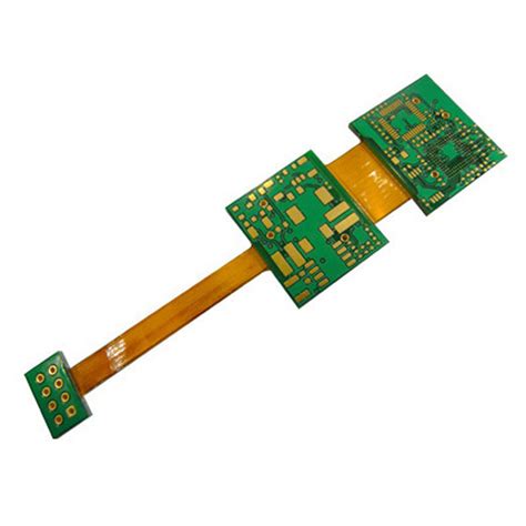
Flex-Rigid PCBs, also known as rigid-flex PCBs, are a combination of flexible and rigid printed circuit boards that offer the best of both worlds. They consist of multiple layers of flexible PCB substrate that are bonded together with rigid PCB sections, creating a single circuit that can be bent, folded, or twisted as needed. This unique design enables electronics manufacturers to create more compact, lightweight, and reliable devices that can withstand harsh environments and repeated flexing.
Flex-Rigid PCBs are increasingly used in various industries, including aerospace, military, medical, automotive, and consumer electronics. They offer several advantages over traditional rigid PCBs, such as:
- Reduced size and weight
- Improved reliability and durability
- Increased design flexibility
- Simplified assembly process
- Better signal integrity and EMI shielding
However, the assembly of Flex-Rigid PCBs can be challenging due to their complex structure and delicate nature. In this article, we will discuss some best practices and techniques to make the assembly of Flex-Rigid PCBs simpler and more reliable.
Understanding the Structure of Flex-Rigid PCB
Before we dive into the assembly process, let’s first understand the basic structure of a Flex-Rigid PCB. A typical Flex-Rigid PCB consists of the following layers:
- Coverlay: A protective layer that covers the outer surfaces of the flexible sections to prevent damage and provide insulation.
- Flexible Substrate: A thin, flexible dielectric material, such as polyimide or polyester, that provides the base for the flexible sections.
- Adhesive: A bonding material that holds the flexible and rigid sections together.
- Rigid Substrate: A standard rigid PCB material, such as FR-4, that provides the base for the rigid sections.
- Copper Traces: Conductive paths that carry electrical signals between components.
- Vias: Conductive holes that connect different layers of the PCB.
- Components: Electronic parts, such as resistors, capacitors, and ICs, that are mounted on the PCB.
The number and arrangement of these layers can vary depending on the specific design requirements of the Flex-Rigid PCB.

Design Considerations for Flex-Rigid PCB Assembly
To ensure a successful and reliable assembly of Flex-Rigid PCBs, it is essential to consider the following design factors:
Bend Radius and Flex Cycles
The bend radius and the number of flex cycles are critical parameters that determine the reliability and durability of Flex-Rigid PCBs. The bend radius refers to the minimum radius that the flexible sections can be bent without causing damage to the copper traces or the substrate. The number of flex cycles refers to the number of times the flexible sections can be bent and straightened without failing.
To minimize stress and prevent failures, it is recommended to:
- Use a larger bend radius whenever possible, typically at least 10 times the thickness of the flexible substrate.
- Avoid sharp bends or creases that can cause cracks or delamination.
- Use strain relief features, such as slots or cut-outs, to reduce stress at the transition points between flexible and rigid sections.
- Specify the expected number of flex cycles and test the design accordingly.
Copper Thickness and Trace Width
The thickness of the copper traces and their width can affect the flexibility and signal integrity of Flex-Rigid PCBs. Thinner copper traces are more flexible but have higher resistance and are more prone to breakage. Wider traces can carry more current but may reduce the flexibility and increase the overall size of the PCB.
To optimize the design, it is recommended to:
- Use thinner copper traces (typically 1/2 oz or 0.5 mil) for the flexible sections and thicker traces (1 oz or 1 mil) for the rigid sections.
- Use wider traces for power and ground connections and narrower traces for signal connections.
- Maintain a consistent trace width and spacing throughout the design to avoid impedance mismatches and signal reflections.
- Use copper poured planes or hatched polygons instead of solid planes to improve flexibility.
Coverlay and Stiffener Materials
The choice of coverlay and stiffener materials can impact the durability, flexibility, and environmental resistance of Flex-Rigid PCBs. The coverlay is typically made of polyimide or polyester and provides a protective barrier against moisture, chemicals, and abrasion. The stiffener is usually made of FR-4 or polyimide and provides additional support and rigidity to the flexible sections.
To select the right materials, it is recommended to:
- Use high-quality, UL-rated coverlay materials that meet the specific requirements of the application, such as temperature range, flame retardancy, and chemical resistance.
- Use thinner and more flexible coverlays for dynamic flexing applications and thicker and more rigid coverlays for static flexing applications.
- Use stiffeners only where necessary to prevent excessive bending or twisting of the flexible sections.
- Use adhesive materials that are compatible with the coverlay and substrate materials and provide strong, reliable bonding.
Via Design and Placement
Vias are critical components in Flex-Rigid PCBs that provide electrical connections between different layers. However, vias can also introduce stress points and potential failure modes if not designed and placed properly.
To optimize via design and placement, it is recommended to:
- Use smaller vias (typically 8-10 mil) to reduce stress concentration and improve flexibility.
- Use via pads with a larger diameter than the via hole to provide additional support and prevent cracking.
- Avoid placing vias in high-stress areas, such as bend regions or transition points between flexible and rigid sections.
- Use teardrops or filleted pads to reinforce the via-to-trace connections and prevent pad lifting or delamination.
- Use conductive microvias or buried vias to reduce the overall thickness of the PCB and improve signal integrity.

Assembly Process for Flex-Rigid PCB
The assembly process for Flex-Rigid PCBs is similar to that of rigid PCBs, but with some additional considerations and precautions to ensure the integrity and reliability of the flexible sections.
Solder Paste Application
Solder paste is a mixture of powdered solder and flux that is used to form electrical and mechanical connections between components and the PCB. The solder paste is typically applied to the PCB using a stencil printer or a dispensing system.
For Flex-Rigid PCBs, it is recommended to:
- Use a thinner stencil (typically 4-5 mil) to reduce the amount of solder paste and prevent bridging or slumping.
- Use a fine-pitch stencil aperture to ensure precise and consistent solder paste deposition.
- Use a low-temperature solder paste (such as Sn42/Bi58 or SnBiAg) to reduce the thermal stress on the flexible sections during reflow.
- Use a nitrogen reflow oven to minimize oxidation and improve wetting.
Component Placement
Component placement is the process of positioning and aligning the electronic components on the PCB before soldering. For Flex-Rigid PCBs, it is essential to ensure that the components are placed accurately and securely, especially on the flexible sections.
To optimize component placement, it is recommended to:
- Use a pick-and-place machine with vision alignment and force feedback to ensure precise and gentle placement.
- Use a flexible nozzle or gripper to handle the components without damaging the flexible substrate.
- Use a placement pressure of 1-2 N and a placement speed of 50-100 mm/s to avoid excessive stress on the components and the PCB.
- Use a placement accuracy of ±50 μm or better to ensure reliable soldering and prevent misalignment.
- Use a conformal coating or underfill material to provide additional support and protection for the components on the flexible sections.
Soldering and Reflow
Soldering is the process of melting the solder paste to form a permanent connection between the components and the PCB. Reflow is the most common method of soldering for Flex-Rigid PCBs, where the entire assembly is heated in an oven to melt the solder paste and form the joints.
To optimize soldering and reflow, it is recommended to:
- Use a low-temperature solder paste and a gentle reflow profile to minimize thermal stress and prevent delamination or warpage.
- Use a peak temperature of 220-240°C and a time above liquidus (TAL) of 60-90 seconds for lead-free solder pastes.
- Use a ramp rate of 2-3°C/second and a cooling rate of 4-6°C/second to avoid thermal shock and ensure proper solidification.
- Use a nitrogen reflow oven with oxygen levels below 100 ppm to prevent oxidation and improve joint quality.
- Use a visual inspection system or X-ray machine to verify the solder joint quality and detect any defects or voids.
Cleaning and Inspection
Cleaning is the process of removing any residual flux or contaminants from the PCB after soldering. Inspection is the process of verifying the quality and reliability of the assembled PCB before final testing and packaging.
For Flex-Rigid PCBs, it is recommended to:
- Use a mild, no-clean flux that does not require aggressive cleaning agents or processes.
- Use an aqueous or semi-aqueous cleaning system with low pressure and temperature to avoid damaging the flexible sections.
- Use a high-resolution inspection system, such as automated optical inspection (AOI) or 3D X-ray, to detect any defects or anomalies in the solder joints, components, or substrate.
- Use a functional testing system to verify the electrical performance and reliability of the assembled PCB under various environmental and mechanical stress conditions.

Troubleshooting Common Issues in Flex-Rigid PCB Assembly
Despite following the best practices and precautions, some issues may still arise during the assembly of Flex-Rigid PCBs. Here are some common issues and their possible solutions:
Delamination or Cracking
Delamination or cracking of the flexible substrate can occur due to excessive bending, thermal stress, or mechanical stress during the assembly process. To prevent or mitigate this issue, it is recommended to:
- Use a larger bend radius and avoid sharp bends or creases in the design.
- Use a low-stress coverlay material and a compatible adhesive material.
- Use a gentle reflow profile and a low-temperature solder paste.
- Use a supporting fixture or carrier to hold the flexible sections during handling and processing.
Solder Joint Defects
Solder joint defects, such as bridging, voiding, or poor wetting, can occur due to improper solder paste application, component placement, or reflow profile. To prevent or mitigate this issue, it is recommended to:
- Use a thinner stencil and a fine-pitch aperture for solder paste application.
- Use a precise and gentle pick-and-place machine for component placement.
- Use a low-temperature solder paste and a gentle reflow profile with a nitrogen atmosphere.
- Use a visual inspection system or X-ray machine to verify the solder joint quality.
Component Shifting or Misalignment
Component shifting or misalignment can occur due to improper placement, vibration, or thermal expansion during the reflow process. To prevent or mitigate this issue, it is recommended to:
- Use a high-accuracy pick-and-place machine with vision alignment and force feedback.
- Use a placement pressure of 1-2 N and a placement speed of 50-100 mm/s.
- Use a conformal coating or underfill material to provide additional support and stability for the components.
- Use a reflow profile with a slow ramp rate and a long soaking zone to allow for uniform heating and expansion.
Signal Integrity or EMI Issues
Signal integrity or EMI issues can occur due to improper trace routing, impedance mismatch, or crosstalk between the flexible and rigid sections of the PCB. To prevent or mitigate this issue, it is recommended to:
- Use a consistent trace width and spacing throughout the design.
- Use a controlled impedance design with matched trace lengths and terminations.
- Use ground planes or shielding layers to reduce crosstalk and EMI.
- Use high-speed materials and low-loss dielectrics for the flexible substrate and coverlay.
- Use signal integrity simulation and testing to verify the performance of the assembled PCB.
Conclusion
Flex-Rigid PCBs offer numerous advantages over traditional rigid PCBs, but their assembly can be challenging and requires careful consideration of design, materials, and processes. By following the best practices and techniques outlined in this article, electronics manufacturers can make the assembly of Flex-Rigid PCBs simpler, more reliable, and more cost-effective.
Some key takeaways from this article include:
- Understanding the basic structure and design considerations of Flex-Rigid PCBs, such as bend radius, copper thickness, coverlay materials, and via placement.
- Optimizing the assembly process, including solder paste application, component placement, soldering and reflow, and cleaning and inspection.
- Troubleshooting common issues in Flex-Rigid PCB assembly, such as delamination, solder joint defects, component shifting, and signal integrity issues.
By mastering these aspects of Flex-Rigid PCB assembly, electronics manufacturers can unlock the full potential of this innovative technology and create more advanced, reliable, and compact devices for a wide range of applications.
Frequently Asked Questions (FAQ)
1. What is the difference between Flex-Rigid PCBs and traditional rigid PCBs?
Flex-Rigid PCBs combine flexible and rigid substrates into a single circuit board, allowing for bending, folding, and twisting of certain sections. This enables more compact, lightweight, and reliable designs compared to traditional rigid PCBs.
2. What are the main advantages of using Flex-Rigid PCBs?
The main advantages of using Flex-Rigid PCBs include reduced size and weight, improved reliability and durability, increased design flexibility, simplified assembly process, and better signal integrity and EMI shielding.
3. What materials are commonly used for the flexible substrate in Flex-Rigid PCBs?
The most common materials used for the flexible substrate in Flex-Rigid PCBs are polyimide (PI) and polyester (PET). These materials offer high flexibility, thermal stability, and electrical insulation properties.
4. What are some key design considerations for Flex-Rigid PCBs?
Some key design considerations for Flex-Rigid PCBs include bend radius and flex cycles, copper thickness and trace width, coverlay and stiffener materials, via design and placement, and signal integrity and EMI control.
5. What are some common issues that can occur during the assembly of Flex-Rigid PCBs, and how can they be prevented or mitigated?
Some common issues that can occur during the assembly of Flex-Rigid PCBs include delamination or cracking of the flexible substrate, solder joint defects, component shifting or misalignment, and signal integrity or EMI issues. These issues can be prevented or mitigated by following best practices in design, materials selection, and assembly processes, such as using a larger bend radius, a low-temperature solder paste, a precise pick-and-place machine, and a gentle reflow profile.
No responses yet